- 您现在的位置:买卖IC网 > PDF目录145822 > BM1301-7PD4H 1-OUTPUT 50 W DC-DC REG PWR SUPPLY MODULE PDF资料下载
参数资料
| 型号: | BM1301-7PD4H |
| 元件分类: | 电源模块 |
| 英文描述: | 1-OUTPUT 50 W DC-DC REG PWR SUPPLY MODULE |
| 封装: | METAL, CASE M02, MODULE |
| 文件页数: | 16/25页 |
| 文件大小: | 569K |
| 代理商: | BM1301-7PD4H |
Cassette Style
DC-DC Converters
M Series
Edition 01/01.2001
23/25
V ACFAIL Signal (VME)
Available for units with
Uo1 = 5.1 V. This option defines an
undervoltage monitoring circuit for the input or the input and
main output voltage equivalent to option D and generates
the ACFAIL signal (V signal) which conforms to the VME
standard. The low state level of the ACFAIL signal is speci-
fied at a sink current of
IV = 48 mA to UV
≤ 0.6 V (open-col-
lector output of a NPN transistor). The pull-up resistor feed-
ing the open-collector output should be placed on the VME
backplane.
After the ACFAIL signal has gone low, the VME standard
requires a hold-up time
th of at least 4 ms before the 5.1 V
output drops to 4.875 V when the 5.1 V output is fully
loaded. This hold-up time
th is provided by the internal input
capacitance. Consequently the working input voltage and
the threshold level
Uti should be adequately above the mini-
mum input voltage
Uimin of the converter so that enough
energy is remaining in the input capacitance. If the input
voltage is below the required level, an external hold-up ca-
pacitor (
Ci ext) should be added.
Formula for threshold level for desired value of
th:
2
Po (th + 0.3 ms) 100
Uti =
––––––––––––––––––––– +
Ui min2
Ci min
η
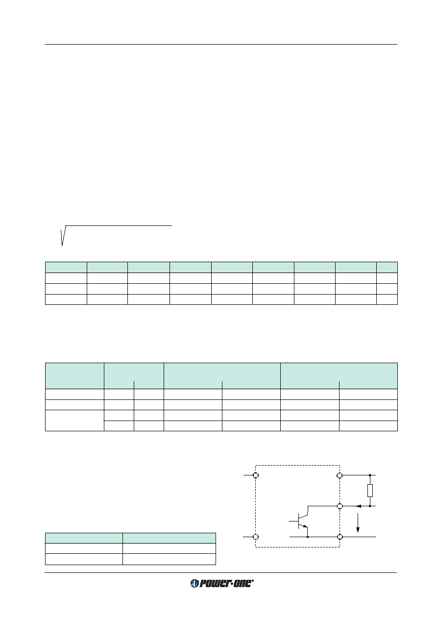
V output (V0, V2, V3):
Connector pin V is internally connected to the open collec-
tor of a NPN transistor. The emitter is connected to the
negative potential of output 1.
UV
≤ 0.6 V (logic low) corre-
sponds to a monitored voltage level (
Ui and/or Uo1) < Ut.
The current
IV through the open collector should not exceed
50 mA. The NPN output is not protected against external
overvoltages.
UV should not exceed 80 V.
Ui, Uo1 status
V output,
UV
Ui or Uo1 < Ut
low, L,
UV ≤ 0.6 V at IV = 50 mA
Ui and Uo1 > Ut + Uh
high, H,
I V ≤ 25 A at UV = 5.1 V
Vo1+
Vo1–
V
UV
IV
Rp
Input
11009
voltage(s) exceed(s)
Ut + Uh. The threshold level Ut is either
adjustable by a potentiometer, accessible through a hole in
the front cover, or is factory adjusted to a determined cus-
tomer specified value.
Versions V0, V2 and V3 are available as shown below.
Option V operates independently of the built-in input under-
voltage lock-out circuit. A logic "low" signal is generated at
pin 5 as soon as one of the monitored voltages drops below
the preselected threshold level
Ut. The return for this signal
is Vo1– (pin 23). The V output recovers when the monitored
Table 22: Undervoltage monitor functions
V output
Monitoring
Minimum adjustment range
Typical hysteresis
Uh [% of Ut]
(VME compatible)
of threshold level
Ut
for
Ut min...Ut max
Ui
Uo1
Uti
Uto
Uhi
Uho
V2
yes
no
Ui min...Ui max 1
–
3.0...0.5
-
V3
yes
Ui min...Ui max 1
0.95...0.98
Uo1 2
3.0...0.5
"0"
V0
yes
no
Ui min...Ui max 3 4
-
2.2...0.4
-
yes
Ui min...Ui max 3 4
0.95...0.98
Uo1 2
2.2...0.4
"0"
1 Threshold level adjustable by potentiometer (not recommended for mobile applications). 2 Fixed value between 95% and 98% of Uo1
(tracking), output undervoltage monitoring is not a requirement of VME standard. 3 Adjusted at
Io nom.
4 Fixed value, resistor-adjusted (
±2% at 25°C) acc. to customer's specifications; individual type number is determined by Power-One.
Table 21: Available internal input capacitance and factory potentiometer setting of Ut i with resulting hold-up time
Types
AM
BM
CM/CMZ
DM/DMZ
EM
FM
LM/LMZ
Unit
Ci min
2.6
0.67
0.37
0.14
0.37
0.14
mF
Ut i
9.5
19.5
39
61
104
39
120
V DC
th
0.34
0.69
1.92
1.73
6.69
2.92
8.18
ms
Fig. 25
Output configuration of options V0, V2 and V3
Formula for additional external input capacitor
2
Po (th + 0.3 ms) 100
Ci ext = ––––––––––––––––––––– – Ci min
η (U
ti
2 – Ui min2)
where as:
Ci min = minimum internal input capacitance [mF], accord-
ing to the table below
Ci ext = external input capacitance [mF]
Po
= output power [W]
η
= efficiency [%]
th
= hold-up time [ms]
Ui min = minimum input voltage [V]
Uti
= threshold level [V]
Remarks: The threshold level
Uti of option V2 and V3 is ad-
justed during manufacture to a value according to the table
below. A decoupling diode should be connected in series
with the input of AM, BM, CM, DM and FM converters to
avoid the input capacitance discharging through other
loads connected to the same source voltage. If LM or LMZ
units are AC powered, an external input capacitor cannot
be applied unless an additional rectifier is provided.
相关PDF资料 |
PDF描述 |
|---|---|
| BM1301-7RD9 | 1-OUTPUT 50 W DC-DC REG PWR SUPPLY MODULE |
| BM1301-7RV0F | 1-OUTPUT 50 W DC-DC REG PWR SUPPLY MODULE |
| BM1301-9PD1HF | 1-OUTPUT 50 W DC-DC REG PWR SUPPLY MODULE |
| BM1301-9PD3AH | 1-OUTPUT 50 W DC-DC REG PWR SUPPLY MODULE |
| BM1501-7PD4 | 1-OUTPUT 50 W DC-DC REG PWR SUPPLY MODULE |
相关代理商/技术参数 |
参数描述 |
|---|---|
| BM1301-7R | 制造商:Power-One 功能描述:DC/DC PS SGL-OUT 12V 4A 50W 11PIN - Bulk |
| BM1301-9R | 制造商:Power-One 功能描述:DC/DC Power Supply Single-OUT 12V 4A 50W 11-Pin 制造商:Power-One 功能描述:ACDC - Bulk |
| BM1-32 | 制造商:SMC 功能描述:Switch mounting band for 32mm cylinder |
| BM1383AGLV-ZE2 | 功能描述:Pressure Sensor 4.35 PSI ~ 15.95 PSI (30 kPa ~ 110 kPa) Absolute 16 b 12-VFLGA 制造商:rohm semiconductor 系列:- 零件状态:在售 压力类型:绝对 工作压力:4.35 PSI ~ 15.95 PSI(30 kPa ~ 110 kPa) 输出类型:I2C 输出:16 b 精度:±1% 电压 - 电源:1.7 V ~ 3.6 V 端口尺寸:- 端口样式:无端口 特性:温度补偿 端子类型:SMD(SMT)接片 最高压力:290.07 PSI(2000 kPa) 工作温度:-40°C ~ 85°C 封装/外壳:12-VFLGA 供应商器件封装:CLGA12V025M 标准包装:1 |
| BM1386GLV-ZTR | 功能描述:PIEZO-RESISTIVE PRESSURE SENSOR, 制造商:rohm semiconductor 系列:- 零件状态:在售 压力类型:绝对 输出类型:I2C 输出:- 精度:±1% 电压 - 电源:1.7 V ~ 3.6 V 端口尺寸:- 端口样式:无端口 特性:温度补偿 端子类型:焊接垫 最高压力:290 PSI (2000 kPa) 工作温度:-40°C ~ 85°C 封装/外壳:10-VFLGA 供应商器件封装:CLGA10V020A 标准包装:1 |
发布紧急采购,3分钟左右您将得到回复。