- 您现在的位置:买卖IC网 > PDF目录210363 > BU-61840B3-102L (DATA DEVICE CORP) 2 CHANNEL(S), 1M bps, MIL-STD-1553 CONTROLLER, PBGA128 PDF资料下载
参数资料
| 型号: | BU-61840B3-102L |
| 厂商: | DATA DEVICE CORP |
| 元件分类: | 微控制器/微处理器 |
| 英文描述: | 2 CHANNEL(S), 1M bps, MIL-STD-1553 CONTROLLER, PBGA128 |
| 封装: | 0.815 X 0.815 INCH, 0.140 INCH HEIGHT, BGA-128 |
| 文件页数: | 44/60页 |
| 文件大小: | 763K |
| 代理商: | BU-61840B3-102L |
第1页第2页第3页第4页第5页第6页第7页第8页第9页第10页第11页第12页第13页第14页第15页第16页第17页第18页第19页第20页第21页第22页第23页第24页第25页第26页第27页第28页第29页第30页第31页第32页第33页第34页第35页第36页第37页第38页第39页第40页第41页第42页第43页当前第44页第45页第46页第47页第48页第49页第50页第51页第52页第53页第54页第55页第56页第57页第58页第59页第60页
49
Data Device Corporation
www.ddc-web.com
BU-6174X/6184X/6186X
D-03/02-250
TRANSPARENT /
BUFFERED
55
Used to select between the buffered mode (when strapped to logic “0”) and transpar-
ent/DMA mode (when strapped to logic “1") for the host processor interface.
B17
IOEN(O)
58
I/O Enable. Tri-state control for external address and data buffers. Generally not used in buffered
mode. When low, indicates that the Enhanced Mini-ACE is currently performing a host access
to an internal register, or internal or (for transparent mode) external RAM. In transparent mode,
IOEN (low) should be used to enable external address and data bus tri-state buffers.
A17
READYD
56
Handshake output to host processor. For a nonzero wait state read access, READYD
is asserted at the end of a host transfer cycle to indicate that data is available to be
read on D15 through D0 when asserted (low). For a nonzero wait state write cycle,
READYD is asserted at the end of the cycle to indicate that data has been transferred
to a register or RAM location. For both nonzero wait reads and writes, the host must
assert STRBD low until READYD is asserted low.
In the (buffered) zero wait state mode, this output is normally logic "1", indicating that the
Enhanced Mini-ACE is in a state ready to accept a subsequent host transfer cycle. In zero
wait mode, READYD will transition from high to low during (or just after) a host transfer
cycle, when the Enhanced Mini-ACE initiates its internal transfer to or from registers or
internal RAM. When the Enhanced Mini-ACE completes its internal transfer, READYD
returns to logic "1", indicating it is ready for the host to initiate a subsequent transfer cycle.
B15
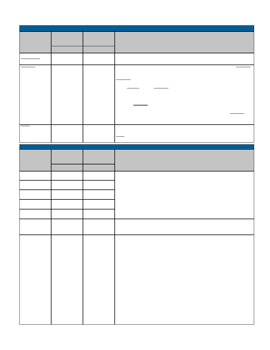
TABLE 51. PROCESSOR INTERFACE CONTROL (CONT.)
SIGNAL NAME
DESCRIPTION
BU-6186XFX/GX
BU-6184XFX/GX
BU-6174XFX/GX
BALL
PIN
BU-61860BX
BU-61840BX
BU-61740BX
RTAD4 (MSB) (I)
35
RT Address inputs. If bit 5 of Configuration Register #6, RT ADDRESS SOURCE, is
programmed to logic "0" (default), then the Enhanced Mini-ACE's RT address is provid-
ed by means of these 5 input signals. In addition, if RT ADDRESS SOURCE is logic
"0", the source of RT address parity is RTADP.
There are many methods for using these input signals for designating the Enhanced
Mini-ACE's RT address. For details, refer to the description of RT_AD_LAT.
If RT ADDRESS SOURCE is programmed to logic "1", then the Enhanced Mini-ACE's
source for its RT address and parity is under software control, via data lines D5-D0. In
this case, the RTAD4-RTAD0 and RTADP signals are not used.
T17
RTAD3 (I)
34
U18
RTAD2 (I)
21
U17
RTAD1 (I)
41
V18
RTAD0 (LSB) (I)
33
V17
RT_AD_LAT (I)
31
RT Address Latch. Input signal used to control the Enhanced MINI-ACE's internal RT
address latch. If RT_AD_LAT is connected to logic "0", then the Enhanced Mini-ACE RT is
configured to accept a hardwired (transparent) RT address from RTAD4-RTAD) and RTADP.
If RT_AD_LAT is initially logic "0", and then transitions to logic "1", the values presented on
RTAD4-RTAD0 and RTADP will be latched internally on the rising edge of RT_AD_LAT.
If RT_AD_LAT is connected to logic "1", then the Enhanced Mini-ACE's RT address is latch-
able under host processor control. In this case, there are two possibilities: (1) If bit 5 of
Configuration Register #6, RT ADDRESS SOURCE, is programmed to logic "0" (default),
then the source of the RT Address is the RTAD4-RTAD0 and RTADP input signals; (2) If RT
ADDRESS SOURCE is programmed to logic "1", then the source of the RT Address is the
lower 6 bits of the processor data bus, D5-D1 (for RTAD4-0) and D0 (for RTADP).
In either of these two cases (with RT_AD_LAT = "1"), the processor will cause the RT
address to be latched by: (1) writing bit 15 of Configuration Register #3, ENHANCED MODE,
to logic "1"; (2) writing bit 3 of Configuration Register #4, LATCH RT ADDRESS WITH CON-
FIGURATION REGISTER #5, to logic "1"; and (3) writing to Configuration Register #5. In the
case of RT ADDRESS SOURCE = "1", then the values of RT address and RT address parity
must be written to the lower 6 bits of Configuration Register #5, via D5-D0. In the case where
RT ADDRESS SOURCE = "0", the bit values presented on D5-D0 become "don't care" .
P18
RTADP
40
Remote Terminal Address Parity. This input signal must provide an odd parity sum with
RTAD4-RTAD0 in order for the RT to respond to non-broadcast commands. That is,
there must be an odd number of logic "1"s from among RTAD-4-RTAD0 and RTADP.
T18
TABLE 52. RT ADDRESS
SIGNAL NAME
DESCRIPTION
BU-6186XFX/GX
BU-6184XFX/GX
BU-6174XFX/GX
BALL
PIN
BU-61860BX
BU-61840BX
BU-61740BX
相关PDF资料 |
PDF描述 |
|---|---|
| BU-61840B3-200L | 2 CHANNEL(S), 1M bps, MIL-STD-1553 CONTROLLER, PBGA128 |
| BU-61840B3-400Y | 2 CHANNEL(S), 1M bps, MIL-STD-1553 CONTROLLER, PBGA128 |
| BU-61840B3-500Q | 2 CHANNEL(S), 1M bps, MIL-STD-1553 CONTROLLER, PBGA128 |
| BU-61840B3-502W | 2 CHANNEL(S), 1M bps, MIL-STD-1553 CONTROLLER, PBGA128 |
| BU-61840B4-500Z | 2 CHANNEL(S), 1M bps, MIL-STD-1553 CONTROLLER, PBGA128 |
相关代理商/技术参数 |
参数描述 |
|---|---|
| BU-61840B3NEW | 制造商:未知厂家 制造商全称:未知厂家 功能描述:MIL-STD-1553 Components |μ-ACE (Micro-ACE?) |
| BU-61843 | 制造商:未知厂家 制造商全称:未知厂家 功能描述:MIL-STD-1553 Components |Enhanced Mini-ACE? |
| BU-61843F3-100 | 制造商:未知厂家 制造商全称:未知厂家 功能描述:Telecommunication IC |
| BU-61843F3-110 | 制造商:未知厂家 制造商全称:未知厂家 功能描述:Telecommunication IC |
| BU-61843F4-100 | 制造商:未知厂家 制造商全称:未知厂家 功能描述:Telecommunication IC |
发布紧急采购,3分钟左右您将得到回复。