参数资料
| 型号: | BU2152FS-E2 |
| 厂商: | Rohm Semiconductor |
| 文件页数: | 4/18页 |
| 文件大小: | 0K |
| 描述: | IC DRVR SER/PAR I/O 24B SSOPA32 |
| 标准包装: | 1 |
| 类型: | 驱动器 |
| 电源电压: | 2.7 V ~ 5.5 V |
| 安装类型: | 表面贴装 |
| 封装/外壳: | 32-SSOP |
| 供应商设备封装: | 32-SSOPA |
| 包装: | 标准包装 |
| 其它名称: | BU2152FS-E2DKR |
BU2050F,BU2092F,BU2092FV,BU2099FV,BD7851FP,BU2152FS
Technical Note
12/24
www.rohm.com
2009.06 - Rev.A
2009 ROHM Co., Ltd. All rights reserved.
【BU2099FV】
●Pin descriptions
Pin No.
Pin Name
I/O
Function
1
VSS
-
GND
2
N.C.
-
Non connected
3
DATA
I
Serial Data Input
4
CLOCK
I
Shift clock of Shift register (Rising Edge Trigger)
5
LCK
I
Latch clock of Storage register (Rising Edge Trigger)
6~17
Q0~Q11
(Qx)
O
Parallel Data Output (Nch Open Drain FET)
Latch Data
L
H
Output FET
ON
OFF
18
SO
O
Serial Data Output
19
OE
I
Output Enable Control Input
*OE pin is pulled down to Vss.
20
VDD
-
Power Supply
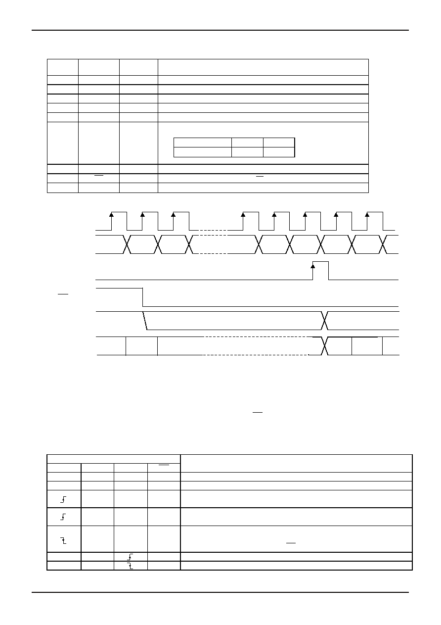
●Timing chart
Fig. 7
1.
After the power is turned on and the voltage is stabilized, LCK should be activates, after clocking 12 data bits into
the DATA terminal.
2.
Qx parallel output data of the shift register is set after the 12
th clock by the LCK.
3.
Since the LCK is a label latch, data is retained in the “L” section and renewed in the “H” section of the LCK.
4.
Data retained in the internal latch circuit is output when the OE is in the “L” section.
5.
The final stage data of the shift register is output to the SO by synchronizing with the rise time of the CLOCK.
[Truth Table]
Input
Function
CLOCK
DATA
LCK
OE
×
H
All the output data output “H” with pull-up.
×
L
The Q0~Q11 output can be enable and output the data of storage register.
L
×
Store “L” in the first stage data of shift register, the previous stage data in the
others. (The conditions of storage register and output have no change.)
H
×
Store “H” in the first stage data of shift register, the previous stage data in the
others. (The conditions of storage register and output have no change.)
×
The data of shift register has no change.
SO outputs the final stage data of shift register with synchronized falling
edge of CLOCK, not controlled by OE.
×
The data of shift register is transferred to the storage register.
×
The data of storage register has no change.
*The Q0~Q11 output have a Nch open drain Tr. The Tr is ON when data from shift register is “L”, and Tr is OFF when data is “H”.
CLOCK
LCK
DATA
DATA12
DATA11
DATA10
DATA2
DATA1
OE
Qx
Previous DATA
DATA
SO
Previous
DATA 11
Previous
DATA 11
DATA12
DATA11
“H”
相关PDF资料 |
PDF描述 |
|---|---|
| BU4551BFV-E2 | IC MUX/DEMUX QUAD 1X2 16SSOP |
| BU4S66G2-TR | IC SWITCH SPST 5SSOP |
| BU6520KV-E2 | IC VIDEO ENCODER AIE 48VQFPC |
| BU7961GUW-E2 | IC TRANSCEIVERS MSDL 63-VBGA |
| BU7962GUW-E2 | IC TRANSCEIVERS MSDL 63-VBGA |
相关代理商/技术参数 |
参数描述 |
|---|---|
| BU2152FV-E2 | 制造商:ROHM 制造商全称:Rohm 功能描述:Serial / Parallel 4-input Drivers |
| BU2173F | 制造商:未知厂家 制造商全称:未知厂家 功能描述:Miscellaneous Clock Generator |
| BU21771 | 制造商:Knowles 功能描述:ACCELEROMETER |
| BU-21771-000 | 功能描述:麦克风 7.92 x 5.59 x 4.14mm ’-45 20hz to 10Khz RoHS:否 制造商:Knowles Acoustics 方向性:Omnidirectional 阻抗:4.4 K Ohms 工作电压:0.9 V to 10 V 灵敏度:- 53 dB 端接类型:Wire Leads 长度:5.56 mm 宽度:3.98 mm 深度:2.21 mm |
| BU-21771-000 | 制造商:Knowles 功能描述:ACCELERATION SENSOR |
发布紧急采购,3分钟左右您将得到回复。