- 您现在的位置:买卖IC网 > PDF目录298892 > BX80526F750256E (INTEL CORP) 32-BIT, 750 MHz, MICROPROCESSOR, PPGA370 PDF资料下载
参数资料
| 型号: | BX80526F750256E |
| 厂商: | INTEL CORP |
| 元件分类: | 微控制器/微处理器 |
| 英文描述: | 32-BIT, 750 MHz, MICROPROCESSOR, PPGA370 |
| 封装: | FCPGA2-370 |
| 文件页数: | 10/94页 |
| 文件大小: | 1014K |
| 代理商: | BX80526F750256E |
第1页第2页第3页第4页第5页第6页第7页第8页第9页当前第10页第11页第12页第13页第14页第15页第16页第17页第18页第19页第20页第21页第22页第23页第24页第25页第26页第27页第28页第29页第30页第31页第32页第33页第34页第35页第36页第37页第38页第39页第40页第41页第42页第43页第44页第45页第46页第47页第48页第49页第50页第51页第52页第53页第54页第55页第56页第57页第58页第59页第60页第61页第62页第63页第64页第65页第66页第67页第68页第69页第70页第71页第72页第73页第74页第75页第76页第77页第78页第79页第80页第81页第82页第83页第84页第85页第86页第87页第88页第89页第90页第91页第92页第93页第94页
18
Datasheet
Pentium III Processor for the PGA370 Socket at 500 MHz to 1.13 GHz
(1.5 V/1.25 V) are used to provide an AGTL+/AGTL termination voltage to the processor, and the
VREF inputs are used as the AGTL+/AGTL reference voltage for the processor. Note that not all
VTT inputs must be connected to the VTT supply. Refer to Section 5.4 for more details.
On the motherboard, all VCCCORE pins must be connected to a voltage island (an island is a portion
of a power plane that has been divided, or an entire plane). In addition, the motherboard must
implement the VTT pins as a voltage island or large trace. Similarly, all GND pins must be
connected to a system ground plane.
Three additional power related pins exist on a processors utilizing the PGA370 socket. They are
VCC1.5,VCC2.5 and VCCCMOS.
The VCCCMOS pin provides the CMOS voltage for the pull-up resistors required on the system
platform. A 2.5 V source must be provided to the VCC2.5 pin and a 1.5 V source must be provided
to the VCC1.5 pin. The source for VCC1.5 must be the same as the one supplying VTT. The processor
routes the compatible CMOS voltage source (1.5 V or 2.5 V) through the package and out to the
VCCCMOS output pin. Processors based on 0.25 micron technology (e.g., the Celeron processor)
utilize 2.5 V CMOS buffers. Processors based on 0.18 micron technology (e.g., the Pentium III
processor for the PGA370 socket) utilize 1.5 V CMOS buffers. The signal VCOREDET can be used
by hardware on the motherboard to detect which CMOS voltage the processor requires. A
VCOREDET connected to VSS within the processor indicates a 1.5 V requirement on VCCCMOS.
Refer to Figure 5.
Each power signal must meet the specifications stated in Table 7 on page 28.
2.3.1
Phase Lock Loop (PLL) Power
It is highly critical that phase lock loop power delivery to the processor meets Intel’s requirements.
A low pass filter is required for power delivery to pins PLL1 and PLL2. This serves as an isolated,
decoupled power source for the internal PLL. Please refer to the Phase Lock Loop Power section in
the appropriate platform design guide for the recommended filter specifications.
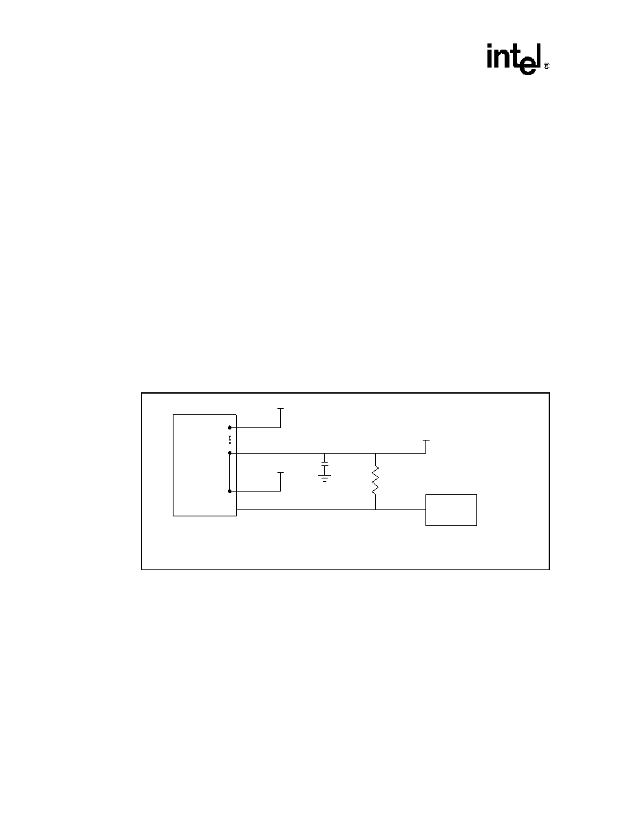
Figure 5. Processor VCCCMOS Package Routing
Intel
Pentium III
Processor
0.1 uF
2.5V Supply
2.5V
1.5V Supply
1.5V
VCC
CMOS
*ICH or
Other Logic
CMOS
Pullups
CMOS Signals
Note: *Ensure this logic is compatible
with 1.5V signal levels of the
Intel Pentium III processor
for the PGA370 socket.
相关PDF资料 |
PDF描述 |
|---|---|
| BX80526F850256E | 32-BIT, 850 MHz, MICROPROCESSOR, PPGA370 |
| BX80526C866256E | 32-BIT, 866 MHz, MICROPROCESSOR, PPGA370 |
| BX80526F733256E | 32-BIT, 733 MHz, MICROPROCESSOR, PPGA370 |
| BX80547RE2533CN | 32-BIT, 2530 MHz, MICROPROCESSOR, PBGA775 |
| BX80547RE2667CN | 32-BIT, 2600 MHz, MICROPROCESSOR, PBGA775 |
相关代理商/技术参数 |
参数描述 |
|---|---|
| BX80526H800256E827304 | 制造商:Intel 功能描述:MPU PENTIUM III CISC 64BIT 0.18UM 800MHZ 370PIN FCPGA - Boxed Product (Development Kits) |
| BX80526KY7002M | 制造商:Intel 功能描述:MPU PENTIUM III XEON 64-BIT 0.18UM 700MHZ - Boxed Product (Development Kits) |
| BX80526KY9002M | 制造商:Intel 功能描述:MPU PENTIUM III XEON 64-BIT 0.18UM 900MHZ - Boxed Product (Development Kits) |
| BX80528JK150GR | 制造商:未知厂家 制造商全称:未知厂家 功能描述:Microprocessor |
| BX80528JK150GR2 | 制造商:未知厂家 制造商全称:未知厂家 功能描述:Microprocessor |
发布紧急采购,3分钟左右您将得到回复。