- 您现在的位置:买卖IC网 > PDF目录298893 > BXM80526B700128 (INTEL CORP) 64-BIT, 700 MHz, MICROPROCESSOR, CPGA495 PDF资料下载
参数资料
| 型号: | BXM80526B700128 |
| 厂商: | INTEL CORP |
| 元件分类: | 微控制器/微处理器 |
| 英文描述: | 64-BIT, 700 MHz, MICROPROCESSOR, CPGA495 |
| 封装: | MICRO, PGA2-495 |
| 文件页数: | 14/74页 |
| 文件大小: | 870K |
| 代理商: | BXM80526B700128 |
第1页第2页第3页第4页第5页第6页第7页第8页第9页第10页第11页第12页第13页当前第14页第15页第16页第17页第18页第19页第20页第21页第22页第23页第24页第25页第26页第27页第28页第29页第30页第31页第32页第33页第34页第35页第36页第37页第38页第39页第40页第41页第42页第43页第44页第45页第46页第47页第48页第49页第50页第51页第52页第53页第54页第55页第56页第57页第58页第59页第60页第61页第62页第63页第64页第65页第66页第67页第68页第69页第70页第71页第72页第73页第74页
Mobile Intel Celeron Processor (0.18) in BGA2 and Micro-PGA2 Packages
at 700MHz, 650 MHz, 600 MHz, 550 MHz, 500 MHz, 450 MHz,
Low-voltage 500 MHz, and Low-voltage 400A MHz
Datasheet
Order#-XXX
14
3.3
System Bus Clock and Processor Clocking
The 2.5-V BCLK clock input directly controls the operating speed of the system bus interface. All
system bus timing parameters are specified with respect to the rising edge of the BCLK input. The
mobile Celeron processor core frequency is a multiple of the BCLK frequency. The processor core
frequency is configured during manufacturing. The configured bus ratio is visible to software in
the Power-on configuration register, see Section 7.2 for details.
Multiplying the bus clock frequency is necessary to increase performance while allowing for
easier distribution of signals within the system. Clock multiplication within the processor is
provided by the internal Phase Lock Loop (PLL), which requires a constant frequency BCLK
input. During Reset or on exit from the Deep Sleep state, the PLL requires some amount of time to
acquire the phase of BCLK. This time is called the PLL lock latency, which is specified in
Section 3.6, AC timing parameters T18 and T47.
3.4
Maximum Ratings
Table 8 contains the mobile Celeron processor stress ratings. Functional operation at the absolute
maximum and minimum is neither implied nor guaranteed. The processor should not receive a
clock while subjected to these conditions. Functional operating conditions are provided in the AC
and DC tables. Extended exposure to the maximum ratings may affect device reliability.
Furthermore, although the processor contains protective circuitry to resist damage from static
electric discharge, one should always take precautions to avoid high static voltages or electric
fields.
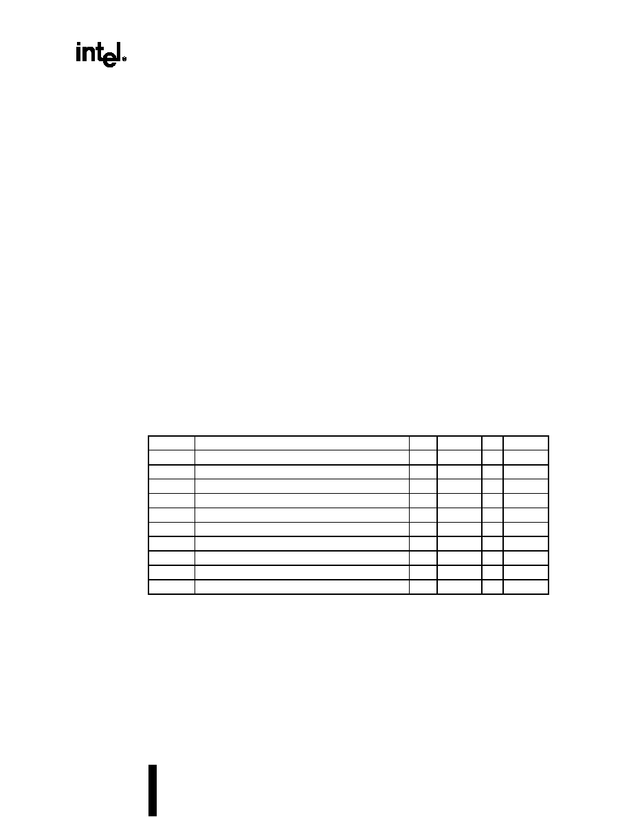
Table 8. Mobile Celeron Processor Absolute Maximum Ratings
Symbol
Parameter
Min
Max
Unit
Notes
TStorage
Storage Temperature
–40
85
°C
Note 1
VCC(Abs)
Supply Voltage with respect to VSS
–0.5
2.1
V
VCCT
System Bus Buffer Voltage with respect to VSS
–0.3
2.1
V
VIN GTL
System Bus Buffer DC Input Voltage with respect to VSS –0.3
2.1
V
Notes 2, 3
VIN GTL
System Bus Buffer DC Input Voltage with respect to VCCT —VCCT + 0.7V V
Notes 2, 4
VIN15
1.5V Buffer DC Input Voltage with respect to VSS
–0.3
2.1
V
Note 5
VIN25
2.5V Buffer DC Input Voltage with respect to VSS
–0.3
3.3
V
Note 6
VIN33
3.3V Buffer DC Input Voltage with respect to VSS
–0.3
3.5
V
Note 7
VINVID
VID ball/pin DC Input Voltage with respect to VSS
—5.5
V
IVID
VID Current
5
mA
Note 8
NOTES:
1.
The shipping container is only rated for 65°C.
2.
Parameter applies to the GTL+ signal groups only. Compliance with both VIN GTL specifications is required.
3.
The voltage on the GTL+ signals must never be below –0.3 or above 2.1V with respect to ground.
4.
The voltage on the GTL+ signals must never be above VCCT + 0.7V even if it is less than VSS + 2.1V, or a short to ground
may occur.
5.
Parameter applies to CMOS, Open-drain, APIC, and TAP bus signal groups only.
6.
Parameter applies to BCLK, CLKREF, PICCLK and PWRGOOD signals.
7.
Parameter applies to BSEL[1:0] signals.
8.
Parameter applies to each VID pin/ball individually.
相关PDF资料 |
PDF描述 |
|---|---|
| BXM80526B700 | 64-BIT, 700 MHz, MICROPROCESSOR, CPGA495 |
| BXM80536GC2100F | 32-BIT, 2100 MHz, MICROPROCESSOR, CPGA478 |
| BXM80536GC1800F | 32-BIT, 1800 MHz, MICROPROCESSOR, CPGA478 |
| BXM80536GC1600F | 32-BIT, 1600 MHz, MICROPROCESSOR, CPGA478 |
| BYP60K4 | 60 A, 400 V, SILICON, RECTIFIER DIODE |
相关代理商/技术参数 |
参数描述 |
|---|---|
| BXM80536NC1400ES L7LS | 制造商:Intel 功能描述:CELERON M,360,1.40GHZ,1M CACHE, 400MHZ FSB,1.26V,UFCPGA - Boxed Product (Development Kits) |
| BXMP1000 | 制造商:SPECTRUM 制造商全称:Spectrum Microwave, Inc. 功能描述:RF AMPLIFIER |
| BXMP1001 | 制造商:SPECTRUM 制造商全称:Spectrum Microwave, Inc. 功能描述:RF AMPLIFIER |
| BXMP1002 | 制造商:SPECTRUM 制造商全称:Spectrum Microwave, Inc. 功能描述:RF AMPLIFIER |
| BXMP1003 | 制造商:SPECTRUM 制造商全称:Spectrum Microwave, Inc. 功能描述:RF AMPLIFIER |
发布紧急采购,3分钟左右您将得到回复。