- 您现在的位置:买卖IC网 > PDF目录298896 > C1851BCU (NEC Corp.) I2C BUS-COMPATIBLE US MTS PROCESSING LSI PDF资料下载
参数资料
| 型号: | C1851BCU |
| 厂商: | NEC Corp. |
| 英文描述: | I2C BUS-COMPATIBLE US MTS PROCESSING LSI |
| 中文描述: | I2C总线兼容美国的多边贸易体制处理LSI |
| 文件页数: | 18/60页 |
| 文件大小: | 447K |
| 代理商: | C1851BCU |
第1页第2页第3页第4页第5页第6页第7页第8页第9页第10页第11页第12页第13页第14页第15页第16页第17页当前第18页第19页第20页第21页第22页第23页第24页第25页第26页第27页第28页第29页第30页第31页第32页第33页第34页第35页第36页第37页第38页第39页第40页第41页第42页第43页第44页第45页第46页第47页第48页第49页第50页第51页第52页第53页第54页第55页第56页第57页第58页第59页第60页
25
PC1851B
Data Sheet S13417EJ2V0DS00
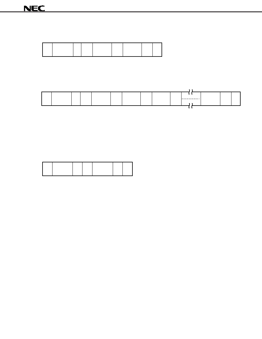
(1) 1-byte data transfer
The format for 1-byte data transfer is the following:
(2) Continuous data transfer
The format when transferring multiple (7) bytes of data at one time by using the automatic increment function is
the following:
The master CPU transfers “00H” as subaddress SA0 following the start condition and slave address. After the
subaddress SA0, the master CPU transfers the SA0 data, and continues with SA1, SA2,..., SAA data without transferring
stop conditions in between. Finally, the stop condition is transferred and the transfer is completed.
(3) Data read
The
PC1851B has one read register. The contents of this register can be read by the master CPU.
The format when data is read is the following:
(4) Acknowledge
In the case of the I2C bus, an acknowledge bit is added to the data as the 9th bit to determine whether data
transfer was successful. The master CPU determines the success or failure of data transfer based on whether this
acknowledge bit is a logical low or high.
If the acknowledge interval is a logical low, this indicates that data transfer was successful. If it is a logical high,
this indicates that data transfer was unsuccessful or that the slave side forcibly released the bus.
Start
Slave
address
Write
mode
Acknow
-ledge
Subaddress
Acknow
-ledge
Data
Acknow
-ledge
Stop
Start
Slave
address
Write
mode
Acknow
-ledge
Subaddress
Acknow
-ledge
Data1
Acknow
-ledge
Data2
Acknow
-ledge
Acknow
-ledge
Stop
Data7
Start
Slave
address
Acknow
-ledge
Data
Non-
acknow
-ledge
Stop
Read
相关PDF资料 |
PDF描述 |
|---|---|
| C1926 | TELECOM TRANSFORMER |
| C1972 | TELECOM TRANSFORMER |
| C200-24308-15-P-C-C | 15 CONTACT(S), MALE, D SUBMINIATURE CONNECTOR, CRIMP |
| C200-24308-15-P-C-N | 15 CONTACT(S), MALE, D SUBMINIATURE CONNECTOR, CRIMP |
| C200-24308-15-P-P-C | 15 CONTACT(S), MALE, D SUBMINIATURE CONNECTOR, SOLDER |
相关代理商/技术参数 |
参数描述 |
|---|---|
| C1854 | 制造商:TE Connectivity 功能描述:TRANSFORMER - Tape and Reel |
| C1854/J | 功能描述:BLOCK 制造商:eaton 系列:* 零件状态:有效 标准包装:1 |
| C1854-J | 制造商:Cooper Bussmann 功能描述:BLOCK - Bulk |
| C1856 | 制造商:TE Connectivity 功能描述:TRANSFORMER - Tape and Reel |
| C1858 | 制造商:n/a 功能描述:_ |
发布紧急采购,3分钟左右您将得到回复。