- 您现在的位置:买卖IC网 > PDF目录11082 > C8051F007-GQR (Silicon Laboratories Inc)IC 8051 MCU 32K FLASH 32LQFP PDF资料下载
参数资料
| 型号: | C8051F007-GQR |
| 厂商: | Silicon Laboratories Inc |
| 文件页数: | 145/171页 |
| 文件大小: | 0K |
| 描述: | IC 8051 MCU 32K FLASH 32LQFP |
| 产品培训模块: | Serial Communication Overview |
| 标准包装: | 500 |
| 系列: | C8051F00x |
| 核心处理器: | 8051 |
| 芯体尺寸: | 8-位 |
| 速度: | 25MHz |
| 连通性: | SMBus(2 线/I²C),SPI,UART/USART |
| 外围设备: | 欠压检测/复位,POR,PWM,温度传感器,WDT |
| 输入/输出数: | 8 |
| 程序存储器容量: | 32KB(32K x 8) |
| 程序存储器类型: | 闪存 |
| RAM 容量: | 2.25K x 8 |
| 电压 - 电源 (Vcc/Vdd): | 2.7 V ~ 3.6 V |
| 数据转换器: | A/D 4x12b; D/A 2x12b |
| 振荡器型: | 内部 |
| 工作温度: | -40°C ~ 85°C |
| 封装/外壳: | 32-LQFP |
| 包装: | 带卷 (TR) |
| 配用: | 336-1188-ND - DEV KIT FOR F005/006/007 |
第1页第2页第3页第4页第5页第6页第7页第8页第9页第10页第11页第12页第13页第14页第15页第16页第17页第18页第19页第20页第21页第22页第23页第24页第25页第26页第27页第28页第29页第30页第31页第32页第33页第34页第35页第36页第37页第38页第39页第40页第41页第42页第43页第44页第45页第46页第47页第48页第49页第50页第51页第52页第53页第54页第55页第56页第57页第58页第59页第60页第61页第62页第63页第64页第65页第66页第67页第68页第69页第70页第71页第72页第73页第74页第75页第76页第77页第78页第79页第80页第81页第82页第83页第84页第85页第86页第87页第88页第89页第90页第91页第92页第93页第94页第95页第96页第97页第98页第99页第100页第101页第102页第103页第104页第105页第106页第107页第108页第109页第110页第111页第112页第113页第114页第115页第116页第117页第118页第119页第120页第121页第122页第123页第124页第125页第126页第127页第128页第129页第130页第131页第132页第133页第134页第135页第136页第137页第138页第139页第140页第141页第142页第143页第144页当前第145页第146页第147页第148页第149页第150页第151页第152页第153页第154页第155页第156页第157页第158页第159页第160页第161页第162页第163页第164页第165页第166页第167页第168页第169页第170页第171页
C8051F000/1/2/5/6/7
C8051F010/1/2/5/6/7
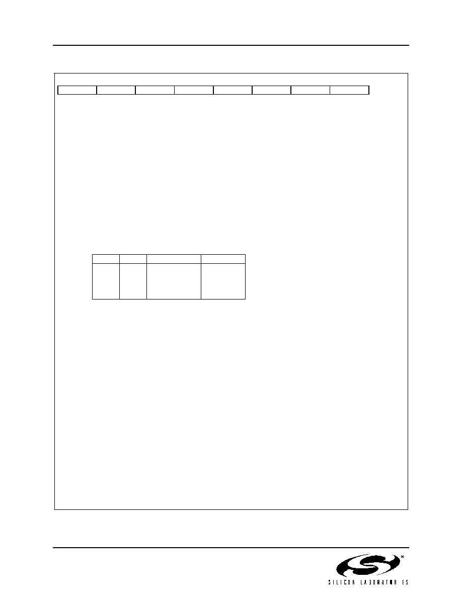
Figure 10.6. PSW: Program Status Word
R/W
Reset Value
CY
AC
F0
RS1
RS0
OV
F1
PARITY
00000000
Bit7
Bit6
Bit5
Bit4
Bit3
Bit2
Bit1
Bit0
SFR Address:
(bit addressable)
0xD0
Bit7:
CY: Carry Flag.
This bit is set when the last arithmetic operation results in a carry (addition) or a borrow
(subtraction). It is cleared to 0 by all other arithmetic operations.
Bit6:
AC: Auxiliary Carry Flag.
This bit is set when the last arithmetic operation results in a carry into (addition) or a
borrow from (subtraction) the high order nibble. It is cleared to 0 by all other arithmetic
operations.
Bit5:
F0: User Flag 0.
This is a bit-addressable, general purpose flag for use under software control.
Bits4-3: RS1-RS0: Register Bank Select.
These bits select which register bank is used during register accesses.
RS1
RS0
Register Bank
Address
0
0x00-0x07
0
1
0x08-0x0F
1
0
2
0x10-0x17
1
3
0x18-0x1F
Note: Any instruction which changes the RS1-RS0 bits must not be immediately followed
by the “MOV Rn, A” instruction.
Bit2:
OV: Overflow Flag.
This bit is set to 1 under the following circumstances:
An ADD, ADDC, or SUBB instruction causes a sign-change overflow.
A MUL instruction results in an overflow (result is greater than 255) .
A DIV instruction causes a divide-by-zero condition.
The OV bit is cleared to 0 by the ADD, ADDC, SUBB, MUL, and DIV instructions in all
other cases.
Bit1:
F1: User Flag 1.
This is a bit-addressable, general purpose flag for use under software control.
Bit0:
PARITY: Parity Flag.
(Read only)
This bit is set to 1 if the sum of the eight bits in the accumulator is odd and cleared if the
sum is even.
75
Rev. 1.7
相关PDF资料 |
PDF描述 |
|---|---|
| VI-25J-CV-B1 | CONVERTER MOD DC/DC 36V 150W |
| VI-24R-CV-B1 | CONVERTER MOD DC/DC 7.5V 150W |
| VI-24N-CV-B1 | CONVERTER MOD DC/DC 18.5V 150W |
| VI-24F-CV-B1 | CONVERTER MOD DC/DC 72V 150W |
| VI-24B-CV-B1 | CONVERTER MOD DC/DC 95V 150W |
相关代理商/技术参数 |
参数描述 |
|---|---|
| C8051F007R | 功能描述:8位微控制器 -MCU C +-12Bit 48Pin RoHS:否 制造商:Silicon Labs 核心:8051 处理器系列:C8051F39x 数据总线宽度:8 bit 最大时钟频率:50 MHz 程序存储器大小:16 KB 数据 RAM 大小:1 KB 片上 ADC:Yes 工作电源电压:1.8 V to 3.6 V 工作温度范围:- 40 C to + 105 C 封装 / 箱体:QFN-20 安装风格:SMD/SMT |
| C8051F007-W | 制造商:Silicon Laboratories Inc 功能描述: |
| C8051F010 | 功能描述:8位微控制器 -MCU 32KB 10ADC RoHS:否 制造商:Silicon Labs 核心:8051 处理器系列:C8051F39x 数据总线宽度:8 bit 最大时钟频率:50 MHz 程序存储器大小:16 KB 数据 RAM 大小:1 KB 片上 ADC:Yes 工作电源电压:1.8 V to 3.6 V 工作温度范围:- 40 C to + 105 C 封装 / 箱体:QFN-20 安装风格:SMD/SMT |
| C8051F010DK | 功能描述:开发板和工具包 - 8051 Dev Kit for F010-12 RoHS:否 制造商:Silicon Labs 产品:Development Kits 工具用于评估:C8051F960, Si7005 核心: 接口类型:USB 工作电源电压: |
| C8051F010-GQ | 功能描述:8位微控制器 -MCU 32KB 10ADC 64P MCU RoHS:否 制造商:Silicon Labs 核心:8051 处理器系列:C8051F39x 数据总线宽度:8 bit 最大时钟频率:50 MHz 程序存储器大小:16 KB 数据 RAM 大小:1 KB 片上 ADC:Yes 工作电源电压:1.8 V to 3.6 V 工作温度范围:- 40 C to + 105 C 封装 / 箱体:QFN-20 安装风格:SMD/SMT |
发布紧急采购,3分钟左右您将得到回复。