- 您现在的位置:买卖IC网 > PDF目录11082 > C8051F007-GQR (Silicon Laboratories Inc)IC 8051 MCU 32K FLASH 32LQFP PDF资料下载
参数资料
| 型号: | C8051F007-GQR |
| 厂商: | Silicon Laboratories Inc |
| 文件页数: | 37/171页 |
| 文件大小: | 0K |
| 描述: | IC 8051 MCU 32K FLASH 32LQFP |
| 产品培训模块: | Serial Communication Overview |
| 标准包装: | 500 |
| 系列: | C8051F00x |
| 核心处理器: | 8051 |
| 芯体尺寸: | 8-位 |
| 速度: | 25MHz |
| 连通性: | SMBus(2 线/I²C),SPI,UART/USART |
| 外围设备: | 欠压检测/复位,POR,PWM,温度传感器,WDT |
| 输入/输出数: | 8 |
| 程序存储器容量: | 32KB(32K x 8) |
| 程序存储器类型: | 闪存 |
| RAM 容量: | 2.25K x 8 |
| 电压 - 电源 (Vcc/Vdd): | 2.7 V ~ 3.6 V |
| 数据转换器: | A/D 4x12b; D/A 2x12b |
| 振荡器型: | 内部 |
| 工作温度: | -40°C ~ 85°C |
| 封装/外壳: | 32-LQFP |
| 包装: | 带卷 (TR) |
| 配用: | 336-1188-ND - DEV KIT FOR F005/006/007 |
第1页第2页第3页第4页第5页第6页第7页第8页第9页第10页第11页第12页第13页第14页第15页第16页第17页第18页第19页第20页第21页第22页第23页第24页第25页第26页第27页第28页第29页第30页第31页第32页第33页第34页第35页第36页当前第37页第38页第39页第40页第41页第42页第43页第44页第45页第46页第47页第48页第49页第50页第51页第52页第53页第54页第55页第56页第57页第58页第59页第60页第61页第62页第63页第64页第65页第66页第67页第68页第69页第70页第71页第72页第73页第74页第75页第76页第77页第78页第79页第80页第81页第82页第83页第84页第85页第86页第87页第88页第89页第90页第91页第92页第93页第94页第95页第96页第97页第98页第99页第100页第101页第102页第103页第104页第105页第106页第107页第108页第109页第110页第111页第112页第113页第114页第115页第116页第117页第118页第119页第120页第121页第122页第123页第124页第125页第126页第127页第128页第129页第130页第131页第132页第133页第134页第135页第136页第137页第138页第139页第140页第141页第142页第143页第144页第145页第146页第147页第148页第149页第150页第151页第152页第153页第154页第155页第156页第157页第158页第159页第160页第161页第162页第163页第164页第165页第166页第167页第168页第169页第170页第171页
C8051F000/1/2/5/6/7
C8051F010/1/2/5/6/7
18.1.
UART Operational Modes
The UART provides four operating modes (one synchronous and three asynchronous) selected by setting
configuration bits in the SCON register. These four modes offer different baud rates and communication protocols.
The four modes are summarized in Table 18.1 below. Detailed descriptions follow.
Table 18.1. UART Modes
Mode
Synchronization
Baud Clock
Data Bits
Start/Stop Bits
0
Synchronous
SYSCLK/12
8
None
1
Asynchronous
Timer 1 or Timer 2 Overflow
8
1 Start, 1 Stop
2
Asynchronous
SYSCLK/32 or SYSCLK/64
9
1 Start, 1 Stop
3
Asynchronous
Timer 1 or Timer 2 Overflow
9
1 Start, 1 Stop
18.1.1. Mode 0: Synchronous Mode
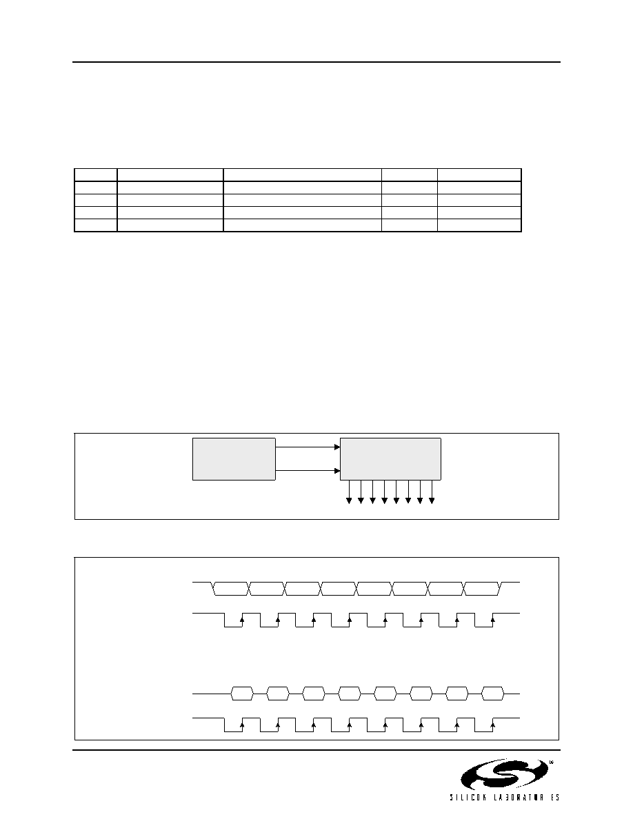
Mode 0 provides synchronous, half-duplex communication. Serial data is transmitted and received on the RX pin.
The TX pin provides the shift clock for both transmit and receive. The MCU must be the master since it generates
the shift clock for transmission in both directions (see the interconnect diagram in Figure 18.2).
Eight data bits are transmitted/received, LSB first (see the timing diagram in Figure 18.3). Data transmission begins
when an instruction writes a data byte to the SBUF register. The TI Transmit Interrupt Flag (SCON.1) is set at the
end of the eighth bit time. Data reception begins when the REN Receive Enable bit (SCON.4) is set to logic 1 and
the RI Receive Interrupt Flag (SCON.0) is cleared. One cycle after the eighth bit is shifted in, the RI flag is set and
reception stops until software clears the RI bit. An interrupt will occur if enabled when either TI or RI is set.
The Mode 0 baud rate is the system clock frequency divided by twelve. RX is forced to open-drain in mode 0, and
an external pull-up will typically be required.
Figure 18.2. UART Mode 0 Interconnect
Shift
Reg.
CLK
C8051Fxxx
RX
TX
DATA
8 Extra Outputs
Figure 18.3. UART Mode 0 Timing Diagram
18.1.2. Mode 1: 8-Bit UART, Variable Baud Rate
D1
D0
D2
D3
D4
D5
D6
D7
RX (data out)
MODE 0 TRANSMIT
D0
MODE 0 RECEIVE
RX (data in)
D1
D2
D3
D4
D5
D6
D7
TX (clk out)
131
Rev. 1.7
相关PDF资料 |
PDF描述 |
|---|---|
| VI-25J-CV-B1 | CONVERTER MOD DC/DC 36V 150W |
| VI-24R-CV-B1 | CONVERTER MOD DC/DC 7.5V 150W |
| VI-24N-CV-B1 | CONVERTER MOD DC/DC 18.5V 150W |
| VI-24F-CV-B1 | CONVERTER MOD DC/DC 72V 150W |
| VI-24B-CV-B1 | CONVERTER MOD DC/DC 95V 150W |
相关代理商/技术参数 |
参数描述 |
|---|---|
| C8051F007R | 功能描述:8位微控制器 -MCU C +-12Bit 48Pin RoHS:否 制造商:Silicon Labs 核心:8051 处理器系列:C8051F39x 数据总线宽度:8 bit 最大时钟频率:50 MHz 程序存储器大小:16 KB 数据 RAM 大小:1 KB 片上 ADC:Yes 工作电源电压:1.8 V to 3.6 V 工作温度范围:- 40 C to + 105 C 封装 / 箱体:QFN-20 安装风格:SMD/SMT |
| C8051F007-W | 制造商:Silicon Laboratories Inc 功能描述: |
| C8051F010 | 功能描述:8位微控制器 -MCU 32KB 10ADC RoHS:否 制造商:Silicon Labs 核心:8051 处理器系列:C8051F39x 数据总线宽度:8 bit 最大时钟频率:50 MHz 程序存储器大小:16 KB 数据 RAM 大小:1 KB 片上 ADC:Yes 工作电源电压:1.8 V to 3.6 V 工作温度范围:- 40 C to + 105 C 封装 / 箱体:QFN-20 安装风格:SMD/SMT |
| C8051F010DK | 功能描述:开发板和工具包 - 8051 Dev Kit for F010-12 RoHS:否 制造商:Silicon Labs 产品:Development Kits 工具用于评估:C8051F960, Si7005 核心: 接口类型:USB 工作电源电压: |
| C8051F010-GQ | 功能描述:8位微控制器 -MCU 32KB 10ADC 64P MCU RoHS:否 制造商:Silicon Labs 核心:8051 处理器系列:C8051F39x 数据总线宽度:8 bit 最大时钟频率:50 MHz 程序存储器大小:16 KB 数据 RAM 大小:1 KB 片上 ADC:Yes 工作电源电压:1.8 V to 3.6 V 工作温度范围:- 40 C to + 105 C 封装 / 箱体:QFN-20 安装风格:SMD/SMT |
发布紧急采购,3分钟左右您将得到回复。