- 您现在的位置:买卖IC网 > PDF目录11083 > C8051F016-GQR (Silicon Laboratories Inc)IC 8051 MCU 32K FLASH 48TQFP PDF资料下载
参数资料
| 型号: | C8051F016-GQR |
| 厂商: | Silicon Laboratories Inc |
| 文件页数: | 73/171页 |
| 文件大小: | 0K |
| 描述: | IC 8051 MCU 32K FLASH 48TQFP |
| 产品培训模块: | Serial Communication Overview |
| 标准包装: | 500 |
| 系列: | C8051F01x |
| 核心处理器: | 8051 |
| 芯体尺寸: | 8-位 |
| 速度: | 25MHz |
| 连通性: | SMBus(2 线/I²C),SPI,UART/USART |
| 外围设备: | 欠压检测/复位,POR,PWM,温度传感器,WDT |
| 输入/输出数: | 16 |
| 程序存储器容量: | 32KB(32K x 8) |
| 程序存储器类型: | 闪存 |
| RAM 容量: | 2.25K x 8 |
| 电压 - 电源 (Vcc/Vdd): | 2.7 V ~ 3.6 V |
| 数据转换器: | A/D 8x10b; D/A 2x12b |
| 振荡器型: | 内部 |
| 工作温度: | -40°C ~ 85°C |
| 封装/外壳: | 48-TQFP |
| 包装: | 带卷 (TR) |
第1页第2页第3页第4页第5页第6页第7页第8页第9页第10页第11页第12页第13页第14页第15页第16页第17页第18页第19页第20页第21页第22页第23页第24页第25页第26页第27页第28页第29页第30页第31页第32页第33页第34页第35页第36页第37页第38页第39页第40页第41页第42页第43页第44页第45页第46页第47页第48页第49页第50页第51页第52页第53页第54页第55页第56页第57页第58页第59页第60页第61页第62页第63页第64页第65页第66页第67页第68页第69页第70页第71页第72页当前第73页第74页第75页第76页第77页第78页第79页第80页第81页第82页第83页第84页第85页第86页第87页第88页第89页第90页第91页第92页第93页第94页第95页第96页第97页第98页第99页第100页第101页第102页第103页第104页第105页第106页第107页第108页第109页第110页第111页第112页第113页第114页第115页第116页第117页第118页第119页第120页第121页第122页第123页第124页第125页第126页第127页第128页第129页第130页第131页第132页第133页第134页第135页第136页第137页第138页第139页第140页第141页第142页第143页第144页第145页第146页第147页第148页第149页第150页第151页第152页第153页第154页第155页第156页第157页第158页第159页第160页第161页第162页第163页第164页第165页第166页第167页第168页第169页第170页第171页
C8051F000/1/2/5/6/7
C8051F010/1/2/5/6/7
21. JTAG (IEEE 1149.1)
Each MCU has an on-chip JTAG interface and logic to support boundary scan for production and in-system testing,
Flash read and write operations, and non-intrusive in-circuit debug. The JTAG interface is fully compliant with the
IEEE 1149.1 specification. Refer to this specification for detailed descriptions of the Test Interface and Boundary-
Scan Architecture. Access of the JTAG Instruction Register (IR) and Data Registers (DR) are as described in the
Test Access Port and Operation of the IEEE 1149.1 specification.
The JTAG interface is via four dedicated pins on the MCU, which are TCK, TMS, TDI, and TDO. These pins are
all 5V tolerant.
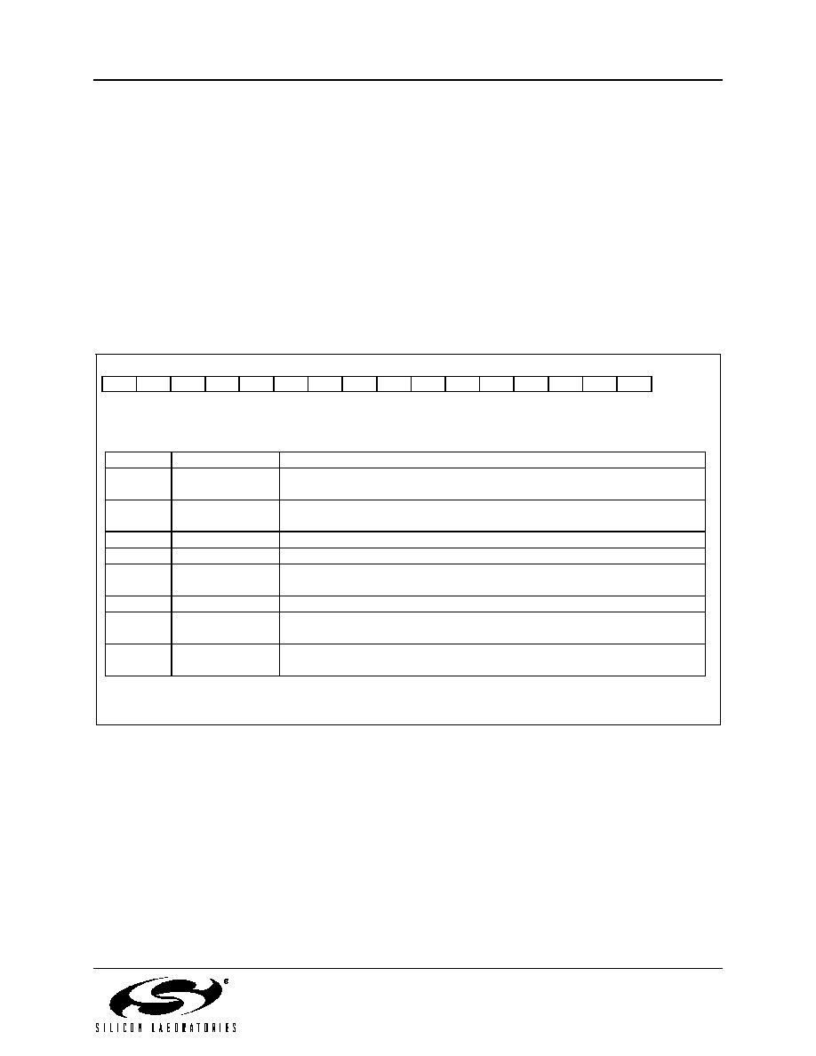
Through the 16-bit JTAG Instruction Register (IR), any of the eight instructions shown in Figure 21.1 can be
commanded. There are three Data Registers (DR’s) associated with JTAG Boundary-Scan, and four associated with
Flash read/write operations on the MCU.
Figure 21.1. IR: JTAG Instruction Register
Reset Value
0x0004
Bit15
Bit0
IR value
Instruction
Description
0x0000
EXTEST
Selects the Boundary Data Register for control and observability of all
device pins
0x0002
SAMPLE/
PRELOAD
Selects the Boundary Data Register for observability and presetting the
scan-path latches
0x0004
IDCODE
Selects device ID Register
0xFFFF
BYPASS
Selects Bypass Data Register
0x0082
Flash Control
Selects FLASHCON Register to control how the interface logic responds to
reads and writes to the FLASHDAT Register
0x0083
Flash Data
Selects FLASHDAT Register for reads and writes to the Flash memory
0x0084
Flash Address
Selects FLASHADR Register which holds the address of all Flash read,
write, and erase operations
0x0085
Flash Scale
Selects FLASHSCL Register which controls the prescaler used to generate
timing signals for Flash operations
Rev. 1.7
164
相关PDF资料 |
PDF描述 |
|---|---|
| C8051F016-GQ | IC 8051 MCU 32K FLASH 48TQFP |
| C8051F041-GQR | IC 8051 MCU 64K FLASH 64TQFP |
| C8051F017-GQR | IC 8051 MCU 32K FLASH 32LQFP |
| C8051F017-GQ | IC 8051 MCU 32K FLASH 32LQFP |
| FIN1022M | IC CROSSPOINT SWITCH 2X2 16SOIC |
相关代理商/技术参数 |
参数描述 |
|---|---|
| C8051F016R | 功能描述:8位微控制器 -MCU C +-10Bit 48Pin RoHS:否 制造商:Silicon Labs 核心:8051 处理器系列:C8051F39x 数据总线宽度:8 bit 最大时钟频率:50 MHz 程序存储器大小:16 KB 数据 RAM 大小:1 KB 片上 ADC:Yes 工作电源电压:1.8 V to 3.6 V 工作温度范围:- 40 C to + 105 C 封装 / 箱体:QFN-20 安装风格:SMD/SMT |
| C8051F017 | 功能描述:8位微控制器 -MCU 32KB 10ADC RoHS:否 制造商:Silicon Labs 核心:8051 处理器系列:C8051F39x 数据总线宽度:8 bit 最大时钟频率:50 MHz 程序存储器大小:16 KB 数据 RAM 大小:1 KB 片上 ADC:Yes 工作电源电压:1.8 V to 3.6 V 工作温度范围:- 40 C to + 105 C 封装 / 箱体:QFN-20 安装风格:SMD/SMT |
| C8051F017-GQ | 功能描述:8位微控制器 -MCU 32KB 10ADC 32P MCU RoHS:否 制造商:Silicon Labs 核心:8051 处理器系列:C8051F39x 数据总线宽度:8 bit 最大时钟频率:50 MHz 程序存储器大小:16 KB 数据 RAM 大小:1 KB 片上 ADC:Yes 工作电源电压:1.8 V to 3.6 V 工作温度范围:- 40 C to + 105 C 封装 / 箱体:QFN-20 安装风格:SMD/SMT |
| C8051F017-GQR | 功能描述:8位微控制器 -MCU 32KB 10ADC 32Pin MCU Tape and Reel RoHS:否 制造商:Silicon Labs 核心:8051 处理器系列:C8051F39x 数据总线宽度:8 bit 最大时钟频率:50 MHz 程序存储器大小:16 KB 数据 RAM 大小:1 KB 片上 ADC:Yes 工作电源电压:1.8 V to 3.6 V 工作温度范围:- 40 C to + 105 C 封装 / 箱体:QFN-20 安装风格:SMD/SMT |
| C8051F017R | 功能描述:8位微控制器 -MCU C +-10Bit 32Pin RoHS:否 制造商:Silicon Labs 核心:8051 处理器系列:C8051F39x 数据总线宽度:8 bit 最大时钟频率:50 MHz 程序存储器大小:16 KB 数据 RAM 大小:1 KB 片上 ADC:Yes 工作电源电压:1.8 V to 3.6 V 工作温度范围:- 40 C to + 105 C 封装 / 箱体:QFN-20 安装风格:SMD/SMT |
发布紧急采购,3分钟左右您将得到回复。