- 您现在的位置:买卖IC网 > PDF目录1907 > C8051F300-GS (Silicon Laboratories Inc)IC 8051 MCU 8K FLASH 14-SOIC PDF资料下载
参数资料
| 型号: | C8051F300-GS |
| 厂商: | Silicon Laboratories Inc |
| 文件页数: | 99/178页 |
| 文件大小: | 0K |
| 描述: | IC 8051 MCU 8K FLASH 14-SOIC |
| 产品培训模块: | Serial Communication Overview |
| 标准包装: | 56 |
| 系列: | C8051F30x |
| 核心处理器: | 8051 |
| 芯体尺寸: | 8-位 |
| 速度: | 25MHz |
| 连通性: | SMBus(2 线/I²C),UART/USART |
| 外围设备: | POR,PWM,温度传感器,WDT |
| 输入/输出数: | 8 |
| 程序存储器容量: | 8KB(8K x 8) |
| 程序存储器类型: | 闪存 |
| RAM 容量: | 256 x 8 |
| 电压 - 电源 (Vcc/Vdd): | 2.7 V ~ 3.6 V |
| 数据转换器: | A/D 8x8b |
| 振荡器型: | 内部 |
| 工作温度: | -40°C ~ 85°C |
| 封装/外壳: | 14-SOIC(0.154",3.90mm 宽) |
| 包装: | 管件 |
| 产品目录页面: | 622 (CN2011-ZH PDF) |
| 配用: | 336-1444-ND - ADAPTER PROGRAM TOOLSTICK F300 336-1351-ND - KIT REF DES TEMP COMPENS RTC 336-1348-ND - KIT STARTER TOOLSTICK 336-1283-ND - KIT REF DESIGN DTMF DECODER 336-1278-ND - KIT TOOL EVAL SYS IN A USB STICK 336-1246-ND - DEV KIT F300/301/302/303/304/305 |
| 其它名称: | 336-1535-5 |
第1页第2页第3页第4页第5页第6页第7页第8页第9页第10页第11页第12页第13页第14页第15页第16页第17页第18页第19页第20页第21页第22页第23页第24页第25页第26页第27页第28页第29页第30页第31页第32页第33页第34页第35页第36页第37页第38页第39页第40页第41页第42页第43页第44页第45页第46页第47页第48页第49页第50页第51页第52页第53页第54页第55页第56页第57页第58页第59页第60页第61页第62页第63页第64页第65页第66页第67页第68页第69页第70页第71页第72页第73页第74页第75页第76页第77页第78页第79页第80页第81页第82页第83页第84页第85页第86页第87页第88页第89页第90页第91页第92页第93页第94页第95页第96页第97页第98页当前第99页第100页第101页第102页第103页第104页第105页第106页第107页第108页第109页第110页第111页第112页第113页第114页第115页第116页第117页第118页第119页第120页第121页第122页第123页第124页第125页第126页第127页第128页第129页第130页第131页第132页第133页第134页第135页第136页第137页第138页第139页第140页第141页第142页第143页第144页第145页第146页第147页第148页第149页第150页第151页第152页第153页第154页第155页第156页第157页第158页第159页第160页第161页第162页第163页第164页第165页第166页第167页第168页第169页第170页第171页第172页第173页第174页第175页第176页第177页第178页
Rev. 2.9
27
C8051F300/1/2/3/4/5
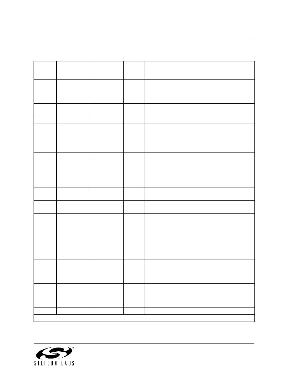
4.
Pinout and Package Definitions
Table 4.1. Pin Definitions for the C8051F300/1/2/3/4/5
Name
Pin
F300/1/2/3/4/5
GM
Pin
F300/1/2/3/4/5
GP
Type
Description
VREF /
P0.0
1
5
A In
D I/O or
A In
External Voltage Reference Input.
Port 0.0. See Section 12 for complete description.
P0.1
2
6
D I/O or
A In
Port 0.1. See Section 12 for complete description.
VDD
3
7
Power Supply Voltage.
XTAL1 /
P0.2
4
8
A In
D I/O or
A In
Crystal Input. This pin is the external oscillator cir-
cuit return for a crystal or ceramic resonator. See
Port 0.2. See Section 12 for complete description.
XTAL2 /
P0.3
5
10
A Out
D I/O
Crystal Input/Output. For an external crystal or res-
onator, this pin is the excitation driver. This pin is
the external clock input for CMOS, capacitor, or RC
network configurations. See Section 11.2.
Port 0.3. See Section 12 for complete description.
P0.4
6
12
D I/O or
A In
Port 0.4. See Section 12 for complete description.
P0.5
7
13
D I/O or
A In
Port 0.5. See Section 12 for complete description.
C2CK /
RST
8
14
D I/O
Clock signal for the C2 Development Interface.
Device Reset. Open-drain output of internal POR or
VDD monitor. An external source can initiate a sys-
tem reset by driving this pin low for at least 10 s.
P0.6 /
CNVSTR
9
1
D I/O or
A In
D I/O
Port 0.6. See Section 12 for complete description.
ADC External Convert Start Input Strobe.
C2D /
P0.7
10
2
D I/O
D I/O or
A In
Data signal for the C2 Development Interface.
Port 0.7. See Section 12 for complete description.
GND
11
3
Ground.
N.C. pins for F30x GP packages: 4, 9, 11
相关PDF资料 |
PDF描述 |
|---|---|
| C8051F310-GQ | IC 8051 MCU 16K FLASH 32LQFP |
| C8051F330-GM | IC 8051 MCU 8K FLASH 20MLP |
| C8051F338-GM | IC MCU 16K FLASH 24QFN |
| C8051F347-GQ | IC 8051 MCU FLASH 32K 32LQFP |
| C8051F350-GQ | IC 8051 MCU 8K FLASH 32LQFP |
相关代理商/技术参数 |
参数描述 |
|---|---|
| C8051F300-GSR | 功能描述:8位微控制器 -MCU 8KB 8ADC 2%osc MCU RoHS:否 制造商:Silicon Labs 核心:8051 处理器系列:C8051F39x 数据总线宽度:8 bit 最大时钟频率:50 MHz 程序存储器大小:16 KB 数据 RAM 大小:1 KB 片上 ADC:Yes 工作电源电压:1.8 V to 3.6 V 工作温度范围:- 40 C to + 105 C 封装 / 箱体:QFN-20 安装风格:SMD/SMT |
| C8051F300P | 功能描述:8位微控制器 -MCU PROTO TYPE VERSION IN 14P DIP PACKAGE RoHS:否 制造商:Silicon Labs 核心:8051 处理器系列:C8051F39x 数据总线宽度:8 bit 最大时钟频率:50 MHz 程序存储器大小:16 KB 数据 RAM 大小:1 KB 片上 ADC:Yes 工作电源电压:1.8 V to 3.6 V 工作温度范围:- 40 C to + 105 C 封装 / 箱体:QFN-20 安装风格:SMD/SMT |
| C8051F300R | 功能描述:8位微控制器 -MCU 8 ADC calOSC RoHS:否 制造商:Silicon Labs 核心:8051 处理器系列:C8051F39x 数据总线宽度:8 bit 最大时钟频率:50 MHz 程序存储器大小:16 KB 数据 RAM 大小:1 KB 片上 ADC:Yes 工作电源电压:1.8 V to 3.6 V 工作温度范围:- 40 C to + 105 C 封装 / 箱体:QFN-20 安装风格:SMD/SMT |
| C8051F300-TB | 功能描述:子卡和OEM板 With C8051F300 MCU RoHS:否 制造商:BeagleBoard by CircuitCo 产品:BeagleBone LCD4 Boards 用于:BeagleBone - BB-Bone - Open Source Development Kit |
| C8051F300-TB-K | 功能描述:BOARD PROTOTYPING W/C8051F300 制造商:silicon labs 系列:- 零件状态:在售 板类型:评估平台 类型:MCU 8-位 核心处理器:8051 操作系统:- 平台:- 配套使用产品/相关产品:C8051F30x 安装类型:固定 内容:板 标准包装:1 |
发布紧急采购,3分钟左右您将得到回复。