- 您现在的位置:买卖IC网 > PDF目录3801 > C8051F301-GS (Silicon Laboratories Inc)IC 8051 MCU 8K FLASH 14-SOIC PDF资料下载
参数资料
| 型号: | C8051F301-GS |
| 厂商: | Silicon Laboratories Inc |
| 文件页数: | 150/178页 |
| 文件大小: | 0K |
| 描述: | IC 8051 MCU 8K FLASH 14-SOIC |
| 产品培训模块: | Serial Communication Overview |
| 标准包装: | 56 |
| 系列: | C8051F30x |
| 核心处理器: | 8051 |
| 芯体尺寸: | 8-位 |
| 速度: | 25MHz |
| 连通性: | SMBus(2 线/I²C),UART/USART |
| 外围设备: | POR,PWM,WDT |
| 输入/输出数: | 8 |
| 程序存储器容量: | 8KB(8K x 8) |
| 程序存储器类型: | 闪存 |
| RAM 容量: | 256 x 8 |
| 电压 - 电源 (Vcc/Vdd): | 2.7 V ~ 3.6 V |
| 振荡器型: | 内部 |
| 工作温度: | -40°C ~ 85°C |
| 封装/外壳: | 14-SOIC(0.154",3.90mm 宽) |
| 包装: | 管件 |
| 产品目录页面: | 622 (CN2011-ZH PDF) |
| 配用: | 336-1444-ND - ADAPTER PROGRAM TOOLSTICK F300 336-1319-ND - REFERENCE DESIGN STEPPER MOTOR |
| 其它名称: | 336-1536-5 |
第1页第2页第3页第4页第5页第6页第7页第8页第9页第10页第11页第12页第13页第14页第15页第16页第17页第18页第19页第20页第21页第22页第23页第24页第25页第26页第27页第28页第29页第30页第31页第32页第33页第34页第35页第36页第37页第38页第39页第40页第41页第42页第43页第44页第45页第46页第47页第48页第49页第50页第51页第52页第53页第54页第55页第56页第57页第58页第59页第60页第61页第62页第63页第64页第65页第66页第67页第68页第69页第70页第71页第72页第73页第74页第75页第76页第77页第78页第79页第80页第81页第82页第83页第84页第85页第86页第87页第88页第89页第90页第91页第92页第93页第94页第95页第96页第97页第98页第99页第100页第101页第102页第103页第104页第105页第106页第107页第108页第109页第110页第111页第112页第113页第114页第115页第116页第117页第118页第119页第120页第121页第122页第123页第124页第125页第126页第127页第128页第129页第130页第131页第132页第133页第134页第135页第136页第137页第138页第139页第140页第141页第142页第143页第144页第145页第146页第147页第148页第149页当前第150页第151页第152页第153页第154页第155页第156页第157页第158页第159页第160页第161页第162页第163页第164页第165页第166页第167页第168页第169页第170页第171页第172页第173页第174页第175页第176页第177页第178页
Rev. 2.9
73
C8051F300/1/2/3/4/5
8.3.2. External Interrupts
The /INT0 and /INT1 external interrupt sources are configurable as active high or low, edge or level sensi-
tive. The IN0PL (/INT0 Polarity) and IN1PL (/INT1 Polarity) bits in the IT01CF register select active high or
active low; the IT0 and IT1 bits in TCON (Section “15.1. Timer 0 and Timer 1” on page 143) select level
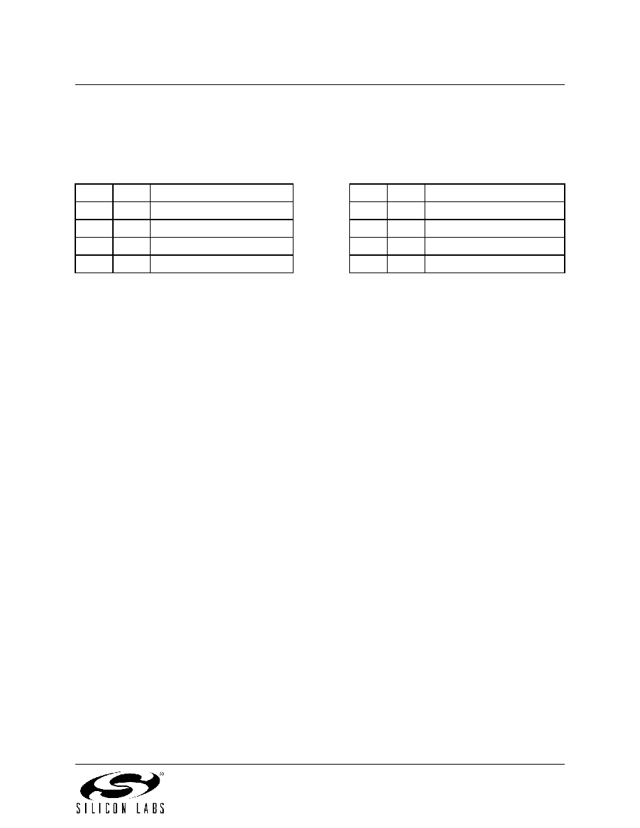
or edge sensitive. The table below lists the possible configurations.
IT0
IN0PL
/INT0 Interrupt
IT1
IN1PL
/INT1 Interrupt
1
0
Active low, edge sensitive
1
Active high, edge sensitive
0
Active low, level sensitive
0
1
Active high, level sensitive
/INT0 and /INT1 are assigned to Port pins as defined in the IT01CF register (see SFR Definition 8.11).
Note that /INT0 and /INT0 Port pin assignments are independent of any Crossbar assignments. /INT0 and
/INT1 will monitor their assigned Port pins without disturbing the peripheral that was assigned the Port pin
via the Crossbar. To assign a Port pin only to /INT0 and/or /INT1, configure the Crossbar to skip the
selected pin(s). This is accomplished by setting the associated bit in register XBR0 (see Section
“12.1. Priority Crossbar Decoder” on page 104 for complete details on configuring the Crossbar).
IE0 (TCON.1) and IE1 (TCON.3) serve as the interrupt-pending flags for the /INT0 and /INT1 external
interrupts, respectively. If an /INT0 or /INT1 external interrupt is configured as edge-sensitive, the corre-
sponding interrupt-pending flag is automatically cleared by the hardware when the CPU vectors to the ISR.
When configured as level sensitive, the interrupt-pending flag remains logic 1 while the input is active as
defined by the corresponding polarity bit (IN0PL or IN1PL); the flag remains logic 0 while the input is inac-
tive. The external interrupt source must hold the input active until the interrupt request is recognized. It
must then deactivate the interrupt request before execution of the ISR completes or another interrupt
request will be generated.
8.3.3. Interrupt Priorities
Each interrupt source can be individually programmed to one of two priority levels: low or high. A low prior-
ity interrupt service routine can be preempted by a high priority interrupt. A high priority interrupt cannot be
preempted. Each interrupt has an associated interrupt priority bit in an SFR (IP or EIP1) used to configure
its priority level. Low priority is the default. If two interrupts are recognized simultaneously, the interrupt with
the higher priority is serviced first. If both interrupts have the same priority level, a fixed priority order is
used to arbitrate, given in Table 8.4.
8.3.4. Interrupt Latency
Interrupt response time depends on the state of the CPU when the interrupt occurs. Pending interrupts are
sampled and priority decoded each system clock cycle. Therefore, the fastest possible response time is 5
system clock cycles: 1 clock cycle to detect the interrupt and 4 clock cycles to complete the LCALL to the
ISR. If an interrupt is pending when a RETI is executed, a single instruction is executed before an LCALL
is made to service the pending interrupt. Therefore, the maximum response time for an interrupt (when no
other interrupt is currently being serviced or the new interrupt is of greater priority) occurs when the CPU is
performing an RETI instruction followed by a DIV as the next instruction. In this case, the response time is
18 system clock cycles: 1 clock cycle to detect the interrupt, 5 clock cycles to execute the RETI, 8 clock
cycles to complete the DIV instruction and 4 clock cycles to execute the LCALL to the ISR. If the CPU is
executing an ISR for an interrupt with equal or higher priority, the new interrupt will not be serviced until the
current ISR completes, including the RETI and following instruction.
10
11
00
01
相关PDF资料 |
PDF描述 |
|---|---|
| C8051F301-GM | IC 8051 MCU 8K FLASH 11QFN |
| 74320-3004 | CONN RCPT VERT ANALOG DGTL DVI |
| 74320-5004 | CONN RCPT VERT ANALOG DGTL DVI |
| C8051F302-GM | IC 8051 MCU 8K FLASH 11QFN |
| C8051F534A-IT | IC 8051 MCU 4K FLASH 20TSSOP |
相关代理商/技术参数 |
参数描述 |
|---|---|
| C8051F301-GSR | 功能描述:8位微控制器 -MCU 8KB 2%osc MCU RoHS:否 制造商:Silicon Labs 核心:8051 处理器系列:C8051F39x 数据总线宽度:8 bit 最大时钟频率:50 MHz 程序存储器大小:16 KB 数据 RAM 大小:1 KB 片上 ADC:Yes 工作电源电压:1.8 V to 3.6 V 工作温度范围:- 40 C to + 105 C 封装 / 箱体:QFN-20 安装风格:SMD/SMT |
| C8051F301R | 功能描述:8位微控制器 -MCU No ADC calOSC RoHS:否 制造商:Silicon Labs 核心:8051 处理器系列:C8051F39x 数据总线宽度:8 bit 最大时钟频率:50 MHz 程序存储器大小:16 KB 数据 RAM 大小:1 KB 片上 ADC:Yes 工作电源电压:1.8 V to 3.6 V 工作温度范围:- 40 C to + 105 C 封装 / 箱体:QFN-20 安装风格:SMD/SMT |
| C8051F302 | 功能描述:8位微控制器 -MCU 8KB 8ADC RoHS:否 制造商:Silicon Labs 核心:8051 处理器系列:C8051F39x 数据总线宽度:8 bit 最大时钟频率:50 MHz 程序存储器大小:16 KB 数据 RAM 大小:1 KB 片上 ADC:Yes 工作电源电压:1.8 V to 3.6 V 工作温度范围:- 40 C to + 105 C 封装 / 箱体:QFN-20 安装风格:SMD/SMT |
| C8051F302-GM | 功能描述:8位微控制器 -MCU 8KB 8ADC 11P MCU RoHS:否 制造商:Silicon Labs 核心:8051 处理器系列:C8051F39x 数据总线宽度:8 bit 最大时钟频率:50 MHz 程序存储器大小:16 KB 数据 RAM 大小:1 KB 片上 ADC:Yes 工作电源电压:1.8 V to 3.6 V 工作温度范围:- 40 C to + 105 C 封装 / 箱体:QFN-20 安装风格:SMD/SMT |
| C8051F302-GMR | 功能描述:8位微控制器 -MCU 8KB 8ADC 11P MCU Tape and Reel RoHS:否 制造商:Silicon Labs 核心:8051 处理器系列:C8051F39x 数据总线宽度:8 bit 最大时钟频率:50 MHz 程序存储器大小:16 KB 数据 RAM 大小:1 KB 片上 ADC:Yes 工作电源电压:1.8 V to 3.6 V 工作温度范围:- 40 C to + 105 C 封装 / 箱体:QFN-20 安装风格:SMD/SMT |
发布紧急采购,3分钟左右您将得到回复。