- 您现在的位置:买卖IC网 > PDF目录3801 > C8051F302-GM (Silicon Laboratories Inc)IC 8051 MCU 8K FLASH 11QFN PDF资料下载
参数资料
| 型号: | C8051F302-GM |
| 厂商: | Silicon Laboratories Inc |
| 文件页数: | 170/178页 |
| 文件大小: | 0K |
| 描述: | IC 8051 MCU 8K FLASH 11QFN |
| 产品培训模块: | Serial Communication Overview |
| 标准包装: | 122 |
| 系列: | C8051F30x |
| 核心处理器: | 8051 |
| 芯体尺寸: | 8-位 |
| 速度: | 25MHz |
| 连通性: | SMBus(2 线/I²C),UART/USART |
| 外围设备: | POR,PWM,温度传感器,WDT |
| 输入/输出数: | 8 |
| 程序存储器容量: | 8KB(8K x 8) |
| 程序存储器类型: | 闪存 |
| RAM 容量: | 256 x 8 |
| 电压 - 电源 (Vcc/Vdd): | 2.7 V ~ 3.6 V |
| 数据转换器: | A/D 8x8b |
| 振荡器型: | 外部 |
| 工作温度: | -40°C ~ 85°C |
| 封装/外壳: | 10-VFDFN 裸露焊盘 |
| 包装: | 管件 |
| 产品目录页面: | 623 (CN2011-ZH PDF) |
| 配用: | 336-1444-ND - ADAPTER PROGRAM TOOLSTICK F300 |
| 其它名称: | 336-1248 |
第1页第2页第3页第4页第5页第6页第7页第8页第9页第10页第11页第12页第13页第14页第15页第16页第17页第18页第19页第20页第21页第22页第23页第24页第25页第26页第27页第28页第29页第30页第31页第32页第33页第34页第35页第36页第37页第38页第39页第40页第41页第42页第43页第44页第45页第46页第47页第48页第49页第50页第51页第52页第53页第54页第55页第56页第57页第58页第59页第60页第61页第62页第63页第64页第65页第66页第67页第68页第69页第70页第71页第72页第73页第74页第75页第76页第77页第78页第79页第80页第81页第82页第83页第84页第85页第86页第87页第88页第89页第90页第91页第92页第93页第94页第95页第96页第97页第98页第99页第100页第101页第102页第103页第104页第105页第106页第107页第108页第109页第110页第111页第112页第113页第114页第115页第116页第117页第118页第119页第120页第121页第122页第123页第124页第125页第126页第127页第128页第129页第130页第131页第132页第133页第134页第135页第136页第137页第138页第139页第140页第141页第142页第143页第144页第145页第146页第147页第148页第149页第150页第151页第152页第153页第154页第155页第156页第157页第158页第159页第160页第161页第162页第163页第164页第165页第166页第167页第168页第169页当前第170页第171页第172页第173页第174页第175页第176页第177页第178页
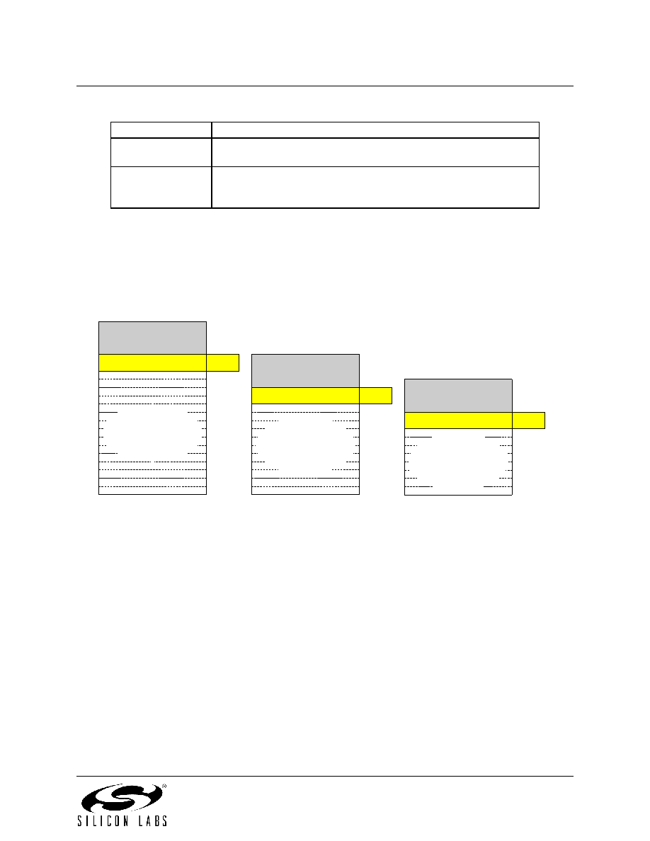
Table 10.2. Security Byte Decoding
Bits
Description
Write Lock: Clearing any of these bits to logic 0 prevents all Flash
memory from being written or page-erased across the C2 interface
Read/Write Lock: Clearing any of these bits to logic 0 prevents all
Flash memory from being read, written, or page-erased across the
C2 interface.
Rev. 2.9
91
C8051F300/1/2/3/4/5
The lock bits can always be read and cleared to logic 0 regardless of the security settings.
Important note: The only means of removing a lock (write or read/write) once set is to erase the
entire program memory space via a C2 Device Erase command.
C8051F300/1/2/3
0x0000
0x1DFF
Lock Byte
Reserved
0x1DFE
FLASH memory
organized in 512-byte
pages
0x1E00
0x0000
0x0FFF
Reserved
0x0FFE
FLASH memory
organized in 512-byte
pages
0x1000
0x0000
0x07FF
Lock Byte
Reserved
0x07FE
FLASH memory
organized in 512-byte
pages
0x0800
Lock Byte
C8051F304
C8051F305
Figure 10.1. Flash Program Memory Map
The level of Flash security depends on the Flash access method. The three Flash access methods that
can be restricted are reads, writes, and erases from the C2 debug interface, user firmware executing on
unlocked pages, and user firmware executing on locked pages.
Accessing Flash from the C2 debug interface:
1.
Any unlocked page may be read, written, or erased.
2.
Locked pages cannot be read, written, or erased.
3.
The page containing the Lock Byte may be read, written, or erased if it is unlocked.
4.
Reading the contents of the Lock Byte is always permitted only if no pages are locked.
5.
Locking additional pages (changing ‘1’s to ‘0’s in the Lock Byte) is not permitted.
6.
Unlocking Flash pages (changing ‘0’s to ‘1’s in the Lock Byte) requires the C2 Device Erase com-
mand, which erases all Flash pages including the page containing the Lock Byte and the Lock
Byte itself.
7.
The Reserved Area cannot be read, written, or erased.
7–4
3–0
相关PDF资料 |
PDF描述 |
|---|---|
| C8051F534A-IT | IC 8051 MCU 4K FLASH 20TSSOP |
| P89LPC915FDH,129 | IC 80C51 MCU FLASH 2K 14-TSSOP |
| C8051F303-GM | IC 8051 MCU 8K FLASH 11QFN |
| AT32UC3C2512C-Z2ZT | IC MCU 32BIT 512KB FLASH 64QFN |
| AU-Y1005-R | CONN USB RTANG FMALE TYPE A PCB |
相关代理商/技术参数 |
参数描述 |
|---|---|
| C8051F302-GMR | 功能描述:8位微控制器 -MCU 8KB 8ADC 11P MCU Tape and Reel RoHS:否 制造商:Silicon Labs 核心:8051 处理器系列:C8051F39x 数据总线宽度:8 bit 最大时钟频率:50 MHz 程序存储器大小:16 KB 数据 RAM 大小:1 KB 片上 ADC:Yes 工作电源电压:1.8 V to 3.6 V 工作温度范围:- 40 C to + 105 C 封装 / 箱体:QFN-20 安装风格:SMD/SMT |
| C8051F302-GS | 功能描述:8位微控制器 -MCU 8KB Flash, 8-bit ADC RoHS:否 制造商:Silicon Labs 核心:8051 处理器系列:C8051F39x 数据总线宽度:8 bit 最大时钟频率:50 MHz 程序存储器大小:16 KB 数据 RAM 大小:1 KB 片上 ADC:Yes 工作电源电压:1.8 V to 3.6 V 工作温度范围:- 40 C to + 105 C 封装 / 箱体:QFN-20 安装风格:SMD/SMT |
| C8051F302-GSR | 功能描述:8位微控制器 -MCU 8KB 8ADC 14Pin MCU RoHS:否 制造商:Silicon Labs 核心:8051 处理器系列:C8051F39x 数据总线宽度:8 bit 最大时钟频率:50 MHz 程序存储器大小:16 KB 数据 RAM 大小:1 KB 片上 ADC:Yes 工作电源电压:1.8 V to 3.6 V 工作温度范围:- 40 C to + 105 C 封装 / 箱体:QFN-20 安装风格:SMD/SMT |
| C8051F302R | 功能描述:8位微控制器 -MCU 8 ADC RoHS:否 制造商:Silicon Labs 核心:8051 处理器系列:C8051F39x 数据总线宽度:8 bit 最大时钟频率:50 MHz 程序存储器大小:16 KB 数据 RAM 大小:1 KB 片上 ADC:Yes 工作电源电压:1.8 V to 3.6 V 工作温度范围:- 40 C to + 105 C 封装 / 箱体:QFN-20 安装风格:SMD/SMT |
| C8051F303 | 功能描述:8位微控制器 -MCU 8KB RoHS:否 制造商:Silicon Labs 核心:8051 处理器系列:C8051F39x 数据总线宽度:8 bit 最大时钟频率:50 MHz 程序存储器大小:16 KB 数据 RAM 大小:1 KB 片上 ADC:Yes 工作电源电压:1.8 V to 3.6 V 工作温度范围:- 40 C to + 105 C 封装 / 箱体:QFN-20 安装风格:SMD/SMT |
发布紧急采购,3分钟左右您将得到回复。