- 您现在的位置:买卖IC网 > PDF目录3801 > C8051F302-GM (Silicon Laboratories Inc)IC 8051 MCU 8K FLASH 11QFN PDF资料下载
参数资料
| 型号: | C8051F302-GM |
| 厂商: | Silicon Laboratories Inc |
| 文件页数: | 83/178页 |
| 文件大小: | 0K |
| 描述: | IC 8051 MCU 8K FLASH 11QFN |
| 产品培训模块: | Serial Communication Overview |
| 标准包装: | 122 |
| 系列: | C8051F30x |
| 核心处理器: | 8051 |
| 芯体尺寸: | 8-位 |
| 速度: | 25MHz |
| 连通性: | SMBus(2 线/I²C),UART/USART |
| 外围设备: | POR,PWM,温度传感器,WDT |
| 输入/输出数: | 8 |
| 程序存储器容量: | 8KB(8K x 8) |
| 程序存储器类型: | 闪存 |
| RAM 容量: | 256 x 8 |
| 电压 - 电源 (Vcc/Vdd): | 2.7 V ~ 3.6 V |
| 数据转换器: | A/D 8x8b |
| 振荡器型: | 外部 |
| 工作温度: | -40°C ~ 85°C |
| 封装/外壳: | 10-VFDFN 裸露焊盘 |
| 包装: | 管件 |
| 产品目录页面: | 623 (CN2011-ZH PDF) |
| 配用: | 336-1444-ND - ADAPTER PROGRAM TOOLSTICK F300 |
| 其它名称: | 336-1248 |
第1页第2页第3页第4页第5页第6页第7页第8页第9页第10页第11页第12页第13页第14页第15页第16页第17页第18页第19页第20页第21页第22页第23页第24页第25页第26页第27页第28页第29页第30页第31页第32页第33页第34页第35页第36页第37页第38页第39页第40页第41页第42页第43页第44页第45页第46页第47页第48页第49页第50页第51页第52页第53页第54页第55页第56页第57页第58页第59页第60页第61页第62页第63页第64页第65页第66页第67页第68页第69页第70页第71页第72页第73页第74页第75页第76页第77页第78页第79页第80页第81页第82页当前第83页第84页第85页第86页第87页第88页第89页第90页第91页第92页第93页第94页第95页第96页第97页第98页第99页第100页第101页第102页第103页第104页第105页第106页第107页第108页第109页第110页第111页第112页第113页第114页第115页第116页第117页第118页第119页第120页第121页第122页第123页第124页第125页第126页第127页第128页第129页第130页第131页第132页第133页第134页第135页第136页第137页第138页第139页第140页第141页第142页第143页第144页第145页第146页第147页第148页第149页第150页第151页第152页第153页第154页第155页第156页第157页第158页第159页第160页第161页第162页第163页第164页第165页第166页第167页第168页第169页第170页第171页第172页第173页第174页第175页第176页第177页第178页
Rev. 2.9
173
C8051F300/1/2/3/4/5
17. C2 Interface
C8051F300/1/2/3/4/5 devices include an on-chip Silicon Labs 2-Wire (C2) debug interface to allow Flash
programming and in-system debugging with the production part installed in the end application. The C2
interface operates using only two pins: a bi-directional data signal (C2D) and a clock input (C2CK). See the
C2 Interface Specification for details on the C2 protocol.
17.1. C2 Interface Registers
The following describes the C2 registers necessary to perform Flash programming functions through the
C2 interface. All C2 registers are accessed through the C2 interface as described in the C2 Interface Spec-
ification.
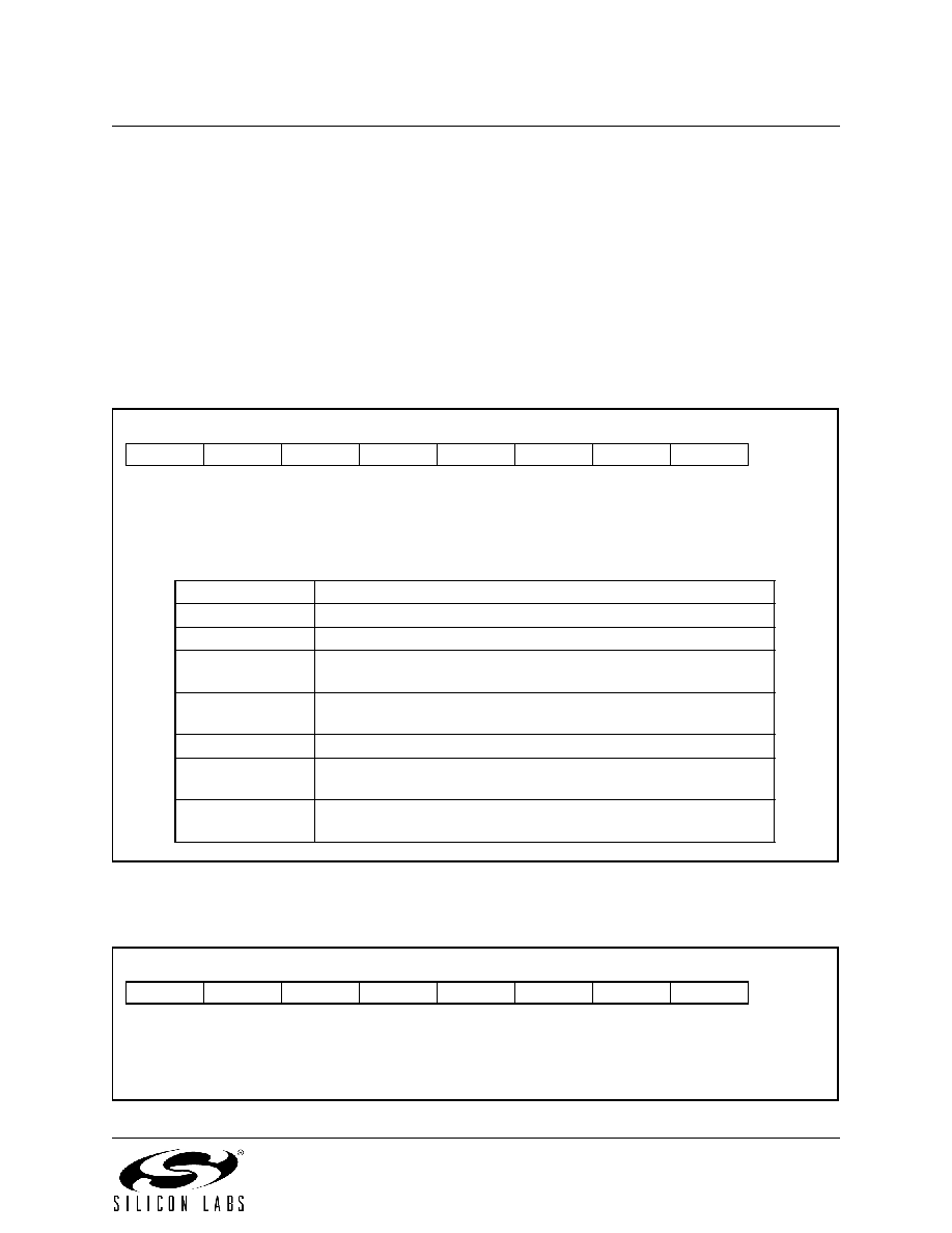
C2 Register Definition 17.1.
Bits7–0: The C2ADD register is accessed via the C2 interface to select the target Data register for
C2 Data Read and Data Write commands.
Reset Value
00000000
Bit7
Bit6
Bit5
Bit4
Bit3
Bit2
Bit1
Bit0
Address
Description
0x00
Selects the Device ID register for Data Read instructions
0x01
Selects the Revision ID register for Data Read instructions
0x02
Selects the C2 Flash Programming Control register for Data
Read/Write instructions
0xB4
Selects the C2 Flash Programming Data register for Data
Read/Write instructions
0x80
Selects the Port0 register for Data Read/Write instructions
0xF1
Selects the Port0 Input Mode register for Data Read/Write instruc-
tions
0xA4
Selects the Port0 Output Mode register for Data Read/Write
instructions
C2ADD: C2 Address
C2 Register Definition 17.2.
This read-only register returns the 8-bit device ID: 0x04 (C8051F300/1/2/3/4/5).
Reset Value
00000100
Bit7
Bit6
Bit5
Bit4
Bit3
Bit2
Bit1
Bit0
DEVICEID: C2 Device ID
相关PDF资料 |
PDF描述 |
|---|---|
| C8051F534A-IT | IC 8051 MCU 4K FLASH 20TSSOP |
| P89LPC915FDH,129 | IC 80C51 MCU FLASH 2K 14-TSSOP |
| C8051F303-GM | IC 8051 MCU 8K FLASH 11QFN |
| AT32UC3C2512C-Z2ZT | IC MCU 32BIT 512KB FLASH 64QFN |
| AU-Y1005-R | CONN USB RTANG FMALE TYPE A PCB |
相关代理商/技术参数 |
参数描述 |
|---|---|
| C8051F302-GMR | 功能描述:8位微控制器 -MCU 8KB 8ADC 11P MCU Tape and Reel RoHS:否 制造商:Silicon Labs 核心:8051 处理器系列:C8051F39x 数据总线宽度:8 bit 最大时钟频率:50 MHz 程序存储器大小:16 KB 数据 RAM 大小:1 KB 片上 ADC:Yes 工作电源电压:1.8 V to 3.6 V 工作温度范围:- 40 C to + 105 C 封装 / 箱体:QFN-20 安装风格:SMD/SMT |
| C8051F302-GS | 功能描述:8位微控制器 -MCU 8KB Flash, 8-bit ADC RoHS:否 制造商:Silicon Labs 核心:8051 处理器系列:C8051F39x 数据总线宽度:8 bit 最大时钟频率:50 MHz 程序存储器大小:16 KB 数据 RAM 大小:1 KB 片上 ADC:Yes 工作电源电压:1.8 V to 3.6 V 工作温度范围:- 40 C to + 105 C 封装 / 箱体:QFN-20 安装风格:SMD/SMT |
| C8051F302-GSR | 功能描述:8位微控制器 -MCU 8KB 8ADC 14Pin MCU RoHS:否 制造商:Silicon Labs 核心:8051 处理器系列:C8051F39x 数据总线宽度:8 bit 最大时钟频率:50 MHz 程序存储器大小:16 KB 数据 RAM 大小:1 KB 片上 ADC:Yes 工作电源电压:1.8 V to 3.6 V 工作温度范围:- 40 C to + 105 C 封装 / 箱体:QFN-20 安装风格:SMD/SMT |
| C8051F302R | 功能描述:8位微控制器 -MCU 8 ADC RoHS:否 制造商:Silicon Labs 核心:8051 处理器系列:C8051F39x 数据总线宽度:8 bit 最大时钟频率:50 MHz 程序存储器大小:16 KB 数据 RAM 大小:1 KB 片上 ADC:Yes 工作电源电压:1.8 V to 3.6 V 工作温度范围:- 40 C to + 105 C 封装 / 箱体:QFN-20 安装风格:SMD/SMT |
| C8051F303 | 功能描述:8位微控制器 -MCU 8KB RoHS:否 制造商:Silicon Labs 核心:8051 处理器系列:C8051F39x 数据总线宽度:8 bit 最大时钟频率:50 MHz 程序存储器大小:16 KB 数据 RAM 大小:1 KB 片上 ADC:Yes 工作电源电压:1.8 V to 3.6 V 工作温度范围:- 40 C to + 105 C 封装 / 箱体:QFN-20 安装风格:SMD/SMT |
发布紧急采购,3分钟左右您将得到回复。