- 您现在的位置:买卖IC网 > PDF目录11175 > C8051F302-GMR (Silicon Laboratories Inc)IC 8051 MCU 8K FLASH 11QFN PDF资料下载
参数资料
| 型号: | C8051F302-GMR |
| 厂商: | Silicon Laboratories Inc |
| 文件页数: | 31/178页 |
| 文件大小: | 0K |
| 描述: | IC 8051 MCU 8K FLASH 11QFN |
| 产品培训模块: | Serial Communication Overview |
| 标准包装: | 1,500 |
| 系列: | C8051F30x |
| 核心处理器: | 8051 |
| 芯体尺寸: | 8-位 |
| 速度: | 25MHz |
| 连通性: | SMBus(2 线/I²C),UART/USART |
| 外围设备: | POR,PWM,温度传感器,WDT |
| 输入/输出数: | 8 |
| 程序存储器容量: | 8KB(8K x 8) |
| 程序存储器类型: | 闪存 |
| RAM 容量: | 256 x 8 |
| 电压 - 电源 (Vcc/Vdd): | 2.7 V ~ 3.6 V |
| 数据转换器: | A/D 8x8b |
| 振荡器型: | 外部 |
| 工作温度: | -40°C ~ 85°C |
| 封装/外壳: | 10-VFDFN 裸露焊盘 |
| 包装: | 带卷 (TR) |
| 配用: | 336-1444-ND - ADAPTER PROGRAM TOOLSTICK F300 |
第1页第2页第3页第4页第5页第6页第7页第8页第9页第10页第11页第12页第13页第14页第15页第16页第17页第18页第19页第20页第21页第22页第23页第24页第25页第26页第27页第28页第29页第30页当前第31页第32页第33页第34页第35页第36页第37页第38页第39页第40页第41页第42页第43页第44页第45页第46页第47页第48页第49页第50页第51页第52页第53页第54页第55页第56页第57页第58页第59页第60页第61页第62页第63页第64页第65页第66页第67页第68页第69页第70页第71页第72页第73页第74页第75页第76页第77页第78页第79页第80页第81页第82页第83页第84页第85页第86页第87页第88页第89页第90页第91页第92页第93页第94页第95页第96页第97页第98页第99页第100页第101页第102页第103页第104页第105页第106页第107页第108页第109页第110页第111页第112页第113页第114页第115页第116页第117页第118页第119页第120页第121页第122页第123页第124页第125页第126页第127页第128页第129页第130页第131页第132页第133页第134页第135页第136页第137页第138页第139页第140页第141页第142页第143页第144页第145页第146页第147页第148页第149页第150页第151页第152页第153页第154页第155页第156页第157页第158页第159页第160页第161页第162页第163页第164页第165页第166页第167页第168页第169页第170页第171页第172页第173页第174页第175页第176页第177页第178页
C8051F300/1/2/3/4/5
126
Rev. 2.9
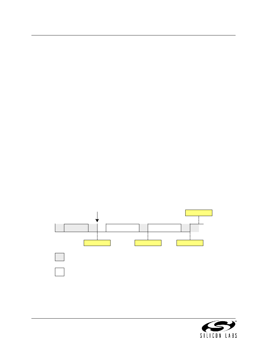
13.5.4. Slave Transmitter Mode
Serial data is transmitted on SDA and the clock is received on SCL. When slave events are enabled (INH
= 0), the interface enters Slave Receiver Mode (to receive the slave address) when a START followed by a
slave address and direction bit (READ in this case) is received. Software responds to the received slave
address with an ACK, or ignores the received slave address with a NACK. If the received address is
ignored, slave interrupts will be inhibited until the next START is detected. If the received slave address is
acknowledged, software should write data to SMB0DAT to force the SMBus into Slave Transmitter Mode.
The switch from Slave Receiver to Slave Transmitter requires software management. Software should per-
form the steps outlined below only when a valid slave address is received (indicated by the label “RX-to-TX
Steps” in Figure 13.8).
Step 1. Set ACK to ‘1’.
Step 2. Write outgoing data to SMB0DAT.
Step 3. Check SMB0DAT.7; if ‘1’, do not perform steps 4, 6 or 7.
Step 4. Set STO to ‘1’.
Step 5. Clear SI to ‘0’.
Step 6. Poll for TXMODE => ‘1’.
Step 7. Clear STO to ‘0’ (must be done before the next ACK cycle).
The interface enters Slave Transmitter Mode and transmits one or more bytes of data (the above steps are
only required before the first byte of the transfer). After each byte is transmitted, the master sends an
acknowledge bit; if the acknowledge bit is an ACK, SMB0DAT should be written with the next data byte. If
the acknowledge bit is a NACK, SMB0DAT should not be written to before SI is cleared (Note: an error
condition may be generated if SMB0DAT is written following a received NACK while in Slave Transmitter
Mode). The interface exits Slave Transmitter Mode after receiving a STOP. Note that the interface will
switch to Slave Receiver Mode if SMB0DAT is not written following a Slave Transmitter interrupt.
Figure 13.8 shows a typical Slave Transmitter sequence. Two transmitted data bytes are shown, though
any number of bytes may be transmitted. Notice that the ‘data byte transferred’ interrupts occur after the
ACK cycle in this mode.
P
R
SLA
S
Data Byte
A
N
A
S = START
P = STOP
N = NACK
W = WRITE
SLA = Slave Address
Received by SMBus
Interface
Transmitted by
SMBus Interface
Interrupt
Perform RX-to-TX
Steps Here
Figure 13.8. Typical Slave Transmitter Sequence
相关PDF资料 |
PDF描述 |
|---|---|
| ISL54051IRUZ-T | IC SWITCH SPST 6UTDFN |
| ISL54054IRUZ-T | IC SWITCH SPST 6UTDFN |
| ISL43L121IUZ-T | IC SWITCH DUAL SPST 8MSOP |
| ISL43L122IUZ-T | IC SWITCH DUAL SPST 8MSOP |
| ISL43L710IUZ-T | IC SWITCH DUAL SPST 8MSOP |
相关代理商/技术参数 |
参数描述 |
|---|---|
| C8051F302-GS | 功能描述:8位微控制器 -MCU 8KB Flash, 8-bit ADC RoHS:否 制造商:Silicon Labs 核心:8051 处理器系列:C8051F39x 数据总线宽度:8 bit 最大时钟频率:50 MHz 程序存储器大小:16 KB 数据 RAM 大小:1 KB 片上 ADC:Yes 工作电源电压:1.8 V to 3.6 V 工作温度范围:- 40 C to + 105 C 封装 / 箱体:QFN-20 安装风格:SMD/SMT |
| C8051F302-GSR | 功能描述:8位微控制器 -MCU 8KB 8ADC 14Pin MCU RoHS:否 制造商:Silicon Labs 核心:8051 处理器系列:C8051F39x 数据总线宽度:8 bit 最大时钟频率:50 MHz 程序存储器大小:16 KB 数据 RAM 大小:1 KB 片上 ADC:Yes 工作电源电压:1.8 V to 3.6 V 工作温度范围:- 40 C to + 105 C 封装 / 箱体:QFN-20 安装风格:SMD/SMT |
| C8051F302R | 功能描述:8位微控制器 -MCU 8 ADC RoHS:否 制造商:Silicon Labs 核心:8051 处理器系列:C8051F39x 数据总线宽度:8 bit 最大时钟频率:50 MHz 程序存储器大小:16 KB 数据 RAM 大小:1 KB 片上 ADC:Yes 工作电源电压:1.8 V to 3.6 V 工作温度范围:- 40 C to + 105 C 封装 / 箱体:QFN-20 安装风格:SMD/SMT |
| C8051F303 | 功能描述:8位微控制器 -MCU 8KB RoHS:否 制造商:Silicon Labs 核心:8051 处理器系列:C8051F39x 数据总线宽度:8 bit 最大时钟频率:50 MHz 程序存储器大小:16 KB 数据 RAM 大小:1 KB 片上 ADC:Yes 工作电源电压:1.8 V to 3.6 V 工作温度范围:- 40 C to + 105 C 封装 / 箱体:QFN-20 安装风格:SMD/SMT |
| C8051F303-GM | 功能描述:8位微控制器 -MCU 8KB 11P MCU RoHS:否 制造商:Silicon Labs 核心:8051 处理器系列:C8051F39x 数据总线宽度:8 bit 最大时钟频率:50 MHz 程序存储器大小:16 KB 数据 RAM 大小:1 KB 片上 ADC:Yes 工作电源电压:1.8 V to 3.6 V 工作温度范围:- 40 C to + 105 C 封装 / 箱体:QFN-20 安装风格:SMD/SMT |
发布紧急采购,3分钟左右您将得到回复。