- 您现在的位置:买卖IC网 > PDF目录11176 > C8051F304-GS (Silicon Laboratories Inc)IC 8051 MCU 4K FLASH 14-SOIC PDF资料下载
参数资料
| 型号: | C8051F304-GS |
| 厂商: | Silicon Laboratories Inc |
| 文件页数: | 21/178页 |
| 文件大小: | 0K |
| 描述: | IC 8051 MCU 4K FLASH 14-SOIC |
| 产品培训模块: | Serial Communication Overview |
| 标准包装: | 56 |
| 系列: | C8051F30x |
| 核心处理器: | 8051 |
| 芯体尺寸: | 8-位 |
| 速度: | 25MHz |
| 连通性: | SMBus(2 线/I²C),UART/USART |
| 外围设备: | POR,PWM,WDT |
| 输入/输出数: | 8 |
| 程序存储器容量: | 4KB(4K x 8) |
| 程序存储器类型: | 闪存 |
| RAM 容量: | 256 x 8 |
| 电压 - 电源 (Vcc/Vdd): | 2.7 V ~ 3.6 V |
| 振荡器型: | 外部 |
| 工作温度: | -40°C ~ 85°C |
| 封装/外壳: | 14-SOIC(0.154",3.90mm 宽) |
| 包装: | 管件 |
| 配用: | 336-1444-ND - ADAPTER PROGRAM TOOLSTICK F300 |
| 其它名称: | 336-1539-5 |
第1页第2页第3页第4页第5页第6页第7页第8页第9页第10页第11页第12页第13页第14页第15页第16页第17页第18页第19页第20页当前第21页第22页第23页第24页第25页第26页第27页第28页第29页第30页第31页第32页第33页第34页第35页第36页第37页第38页第39页第40页第41页第42页第43页第44页第45页第46页第47页第48页第49页第50页第51页第52页第53页第54页第55页第56页第57页第58页第59页第60页第61页第62页第63页第64页第65页第66页第67页第68页第69页第70页第71页第72页第73页第74页第75页第76页第77页第78页第79页第80页第81页第82页第83页第84页第85页第86页第87页第88页第89页第90页第91页第92页第93页第94页第95页第96页第97页第98页第99页第100页第101页第102页第103页第104页第105页第106页第107页第108页第109页第110页第111页第112页第113页第114页第115页第116页第117页第118页第119页第120页第121页第122页第123页第124页第125页第126页第127页第128页第129页第130页第131页第132页第133页第134页第135页第136页第137页第138页第139页第140页第141页第142页第143页第144页第145页第146页第147页第148页第149页第150页第151页第152页第153页第154页第155页第156页第157页第158页第159页第160页第161页第162页第163页第164页第165页第166页第167页第168页第169页第170页第171页第172页第173页第174页第175页第176页第177页第178页
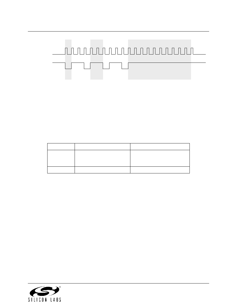
SCL
Timer Source
Overflows
SCL High Timeout
T
Low
T
High
Rev. 2.9
117
C8051F300/1/2/3/4/5
Figure 13.4. Typical SMBus SCL Generation
Setting the EXTHOLD bit extends the minimum setup and hold times for the SDA line. The minimum SDA
setup time defines the absolute minimum time that SDA is stable before SCL transitions from low-to-high.
The minimum SDA hold time defines the absolute minimum time that the current SDA value remains stable
after SCL transitions from high-to-low. EXTHOLD should be set so that the minimum setup and hold times
meet the SMBus Specification requirements of 250 ns and 300 ns, respectively. Table 13.2 shows the min-
imum setup and hold times for the two EXTHOLD settings. Setup and hold time extensions are typically
necessary when SYSCLK is above 10 MHz.
Table 13.2. Minimum SDA Setup and Hold Times
EXTHOLD
Minimum SDA Setup Time
Minimum SDA Hold Time
0
Tlow – 4 system clocks
OR
1 system clock + s/w delay*
3 system clocks
1
11 system clocks
12 system clocks
*Note: Setup Time for ACK bit transmissions and the MSB of all data transfers. The s/w
delay occurs between the time SMB0DAT or ACK is written and when SI is cleared.
Note that if SI is cleared in the same write that defines the outgoing ACK value, s/w
delay is zero.
With the SMBTOE bit set, Timer 2 should be configured to overflow after 25 ms in order to detect SCL low
timeouts (see Section “13.3.3. SCL Low Timeout” on page 114). The SMBus interface will force Timer 2
to reload while SCL is high, and allow Timer 2 to count when SCL is low. The Timer 2 interrupt service rou-
tine should be used to reset SMBus communication by disabling and reenabling the SMBus. Timer 2 con-
figuration is described in Section “15.2. Timer 2” on page 151.
SMBus Free Timeout detection can be enabled by setting the SMBFTE bit. When this bit is set, the bus will
be considered free if SDA and SCL remain high for more than 10 SMBus clock source periods (see
Figure 13.4). When a Free Timeout is detected, the interface will respond as if a STOP was detected (an
interrupt will be generated, and STO will be set).
相关PDF资料 |
PDF描述 |
|---|---|
| VE-JNM-IW-F3 | CONVERTER MOD DC/DC 10V 100W |
| VE-JNM-IW-F2 | CONVERTER MOD DC/DC 10V 100W |
| EFM32TG110F8 | MCU 32BIT 8KB FLASH 24-QFN |
| VE-B6R-IX | CONVERTER MOD DC/DC 7.5V 75W |
| VE-JNL-IW-F4 | CONVERTER MOD DC/DC 28V 100W |
相关代理商/技术参数 |
参数描述 |
|---|---|
| C8051F304-GSR | 功能描述:8位微控制器 -MCU 4KB 14Pin MCU RoHS:否 制造商:Silicon Labs 核心:8051 处理器系列:C8051F39x 数据总线宽度:8 bit 最大时钟频率:50 MHz 程序存储器大小:16 KB 数据 RAM 大小:1 KB 片上 ADC:Yes 工作电源电压:1.8 V to 3.6 V 工作温度范围:- 40 C to + 105 C 封装 / 箱体:QFN-20 安装风格:SMD/SMT |
| C8051F304R | 功能描述:8位微控制器 -MCU 303 4Kbyte RoHS:否 制造商:Silicon Labs 核心:8051 处理器系列:C8051F39x 数据总线宽度:8 bit 最大时钟频率:50 MHz 程序存储器大小:16 KB 数据 RAM 大小:1 KB 片上 ADC:Yes 工作电源电压:1.8 V to 3.6 V 工作温度范围:- 40 C to + 105 C 封装 / 箱体:QFN-20 安装风格:SMD/SMT |
| C8051F305 | 功能描述:8位微控制器 -MCU 2KB RoHS:否 制造商:Silicon Labs 核心:8051 处理器系列:C8051F39x 数据总线宽度:8 bit 最大时钟频率:50 MHz 程序存储器大小:16 KB 数据 RAM 大小:1 KB 片上 ADC:Yes 工作电源电压:1.8 V to 3.6 V 工作温度范围:- 40 C to + 105 C 封装 / 箱体:QFN-20 安装风格:SMD/SMT |
| C8051F305-GM | 功能描述:8位微控制器 -MCU 2KB 11P MCU RoHS:否 制造商:Silicon Labs 核心:8051 处理器系列:C8051F39x 数据总线宽度:8 bit 最大时钟频率:50 MHz 程序存储器大小:16 KB 数据 RAM 大小:1 KB 片上 ADC:Yes 工作电源电压:1.8 V to 3.6 V 工作温度范围:- 40 C to + 105 C 封装 / 箱体:QFN-20 安装风格:SMD/SMT |
| C8051F305-GMR | 功能描述:8位微控制器 -MCU 2KB 11P MCU RoHS:否 制造商:Silicon Labs 核心:8051 处理器系列:C8051F39x 数据总线宽度:8 bit 最大时钟频率:50 MHz 程序存储器大小:16 KB 数据 RAM 大小:1 KB 片上 ADC:Yes 工作电源电压:1.8 V to 3.6 V 工作温度范围:- 40 C to + 105 C 封装 / 箱体:QFN-20 安装风格:SMD/SMT |
发布紧急采购,3分钟左右您将得到回复。