- 您现在的位置:买卖IC网 > PDF目录11176 > C8051F304-GS (Silicon Laboratories Inc)IC 8051 MCU 4K FLASH 14-SOIC PDF资料下载
参数资料
| 型号: | C8051F304-GS |
| 厂商: | Silicon Laboratories Inc |
| 文件页数: | 51/178页 |
| 文件大小: | 0K |
| 描述: | IC 8051 MCU 4K FLASH 14-SOIC |
| 产品培训模块: | Serial Communication Overview |
| 标准包装: | 56 |
| 系列: | C8051F30x |
| 核心处理器: | 8051 |
| 芯体尺寸: | 8-位 |
| 速度: | 25MHz |
| 连通性: | SMBus(2 线/I²C),UART/USART |
| 外围设备: | POR,PWM,WDT |
| 输入/输出数: | 8 |
| 程序存储器容量: | 4KB(4K x 8) |
| 程序存储器类型: | 闪存 |
| RAM 容量: | 256 x 8 |
| 电压 - 电源 (Vcc/Vdd): | 2.7 V ~ 3.6 V |
| 振荡器型: | 外部 |
| 工作温度: | -40°C ~ 85°C |
| 封装/外壳: | 14-SOIC(0.154",3.90mm 宽) |
| 包装: | 管件 |
| 配用: | 336-1444-ND - ADAPTER PROGRAM TOOLSTICK F300 |
| 其它名称: | 336-1539-5 |
第1页第2页第3页第4页第5页第6页第7页第8页第9页第10页第11页第12页第13页第14页第15页第16页第17页第18页第19页第20页第21页第22页第23页第24页第25页第26页第27页第28页第29页第30页第31页第32页第33页第34页第35页第36页第37页第38页第39页第40页第41页第42页第43页第44页第45页第46页第47页第48页第49页第50页当前第51页第52页第53页第54页第55页第56页第57页第58页第59页第60页第61页第62页第63页第64页第65页第66页第67页第68页第69页第70页第71页第72页第73页第74页第75页第76页第77页第78页第79页第80页第81页第82页第83页第84页第85页第86页第87页第88页第89页第90页第91页第92页第93页第94页第95页第96页第97页第98页第99页第100页第101页第102页第103页第104页第105页第106页第107页第108页第109页第110页第111页第112页第113页第114页第115页第116页第117页第118页第119页第120页第121页第122页第123页第124页第125页第126页第127页第128页第129页第130页第131页第132页第133页第134页第135页第136页第137页第138页第139页第140页第141页第142页第143页第144页第145页第146页第147页第148页第149页第150页第151页第152页第153页第154页第155页第156页第157页第158页第159页第160页第161页第162页第163页第164页第165页第166页第167页第168页第169页第170页第171页第172页第173页第174页第175页第176页第177页第178页
C8051F300/1/2/3/4/5
144
Rev. 2.9
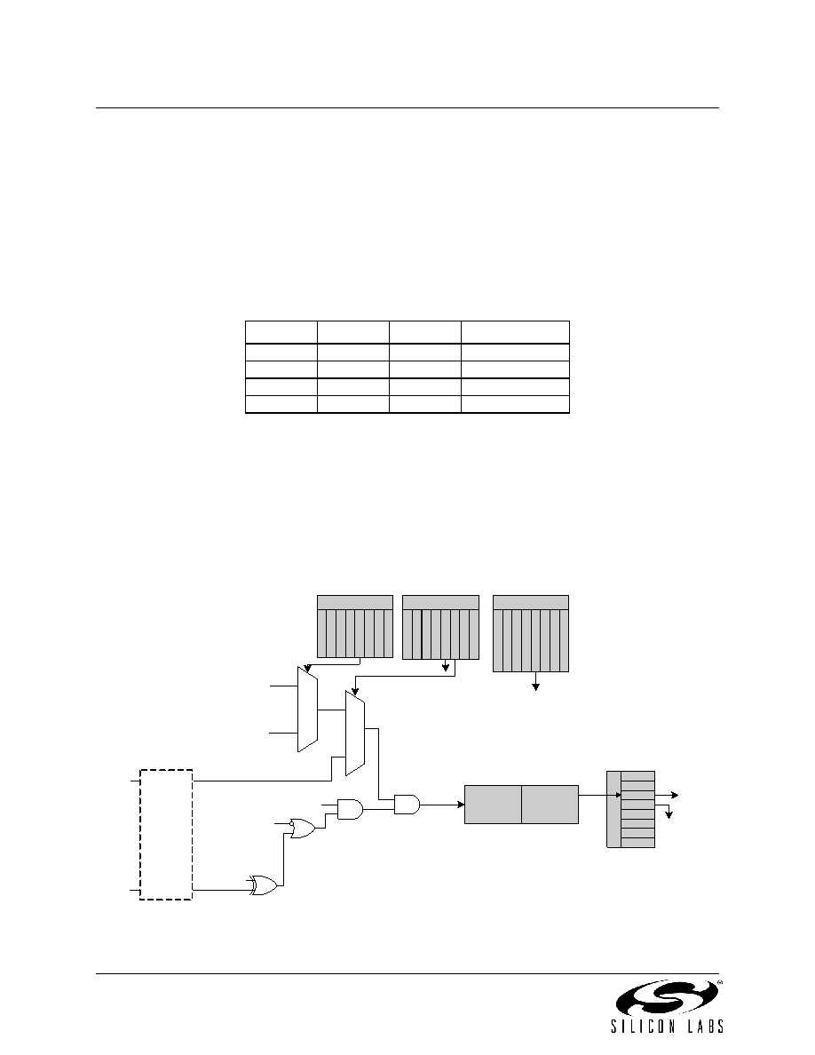
The C/T0 bit (TMOD.2) selects the counter/timer's clock source. When C/T0 is set to logic 1, high-to-low
transitions at the selected Timer 0 input pin (T0) increment the timer register (Refer to Section
“12.1. Priority Crossbar Decoder” on page 104 for information on selecting and configuring external I/O
pins). Clearing C/T selects the clock defined by the T0M bit (CKCON.3). When T0M is set, Timer 0 is
clocked by the system clock. When T0M is cleared, Timer 0 is clocked by the source selected by the Clock
Scale bits in CKCON (see SFR Definition 15.3).
Setting the TR0 bit (TCON.4) enables the timer when either GATE0 (TMOD.3) is logic 0 or the input signal
/INT0 is active as defined by bit IN0PL in register IT01CF (see SFR Definition 8.11). Setting GATE0 to ‘1’
allows the timer to be controlled by the external input signal /INT0 (see Section “8.3.5. Interrupt Register
Descriptions” on page 75), facilitating pulse width measurements.
TR0
GATE0
/INT0
Counter/Timer
*Note: X = Don't Care
Setting TR0 does not force the timer to reset. The timer registers should be loaded with the desired initial
value before the timer is enabled.
TL1 and TH1 form the 13-bit register for Timer 1 in the same manner as described above for TL0 and TH0.
Timer 1 is configured and controlled using the relevant TCON and TMOD bits just as with Timer 0. The
input signal /INT1 is used with Timer 1; the /INT1 polarity is defined by bit IN1PL in register IT01CF (see
TCLK
TL0
(5 bits)
TH0
(8 bits)
TC
O
N
TF0
TR0
TR1
TF1
IE1
IT1
IE0
IT0
Interrupt
TR0
0
1
0
1
SYSCLK
Pre-scaled Clock
CKCON
T
2
M
H
S
C
A
0
S
C
A
1
T
2
M
L
T
1
M
T
0
M
TMOD
T
1
M
1
T
1
M
0
C
/
T
1
G
A
T
E
1
G
A
T
E
0
C
/
T
0
T
0
M
1
T
0
M
0
GATE0
/INT0
T0
Crossbar
IT01CF
I
N
1
S
L
1
I
N
1
S
L
0
I
N
1
S
L
2
I
N
1
P
L
I
N
0
P
L
I
N
0
S
L
2
I
N
0
S
L
1
I
N
0
S
L
0
IN0PL
XOR
Figure 15.1. T0 Mode 0 Block Diagram
0
X*
Disabled
10
X*
Enabled
1
0
Disabled
111
Enabled
相关PDF资料 |
PDF描述 |
|---|---|
| VE-JNM-IW-F3 | CONVERTER MOD DC/DC 10V 100W |
| VE-JNM-IW-F2 | CONVERTER MOD DC/DC 10V 100W |
| EFM32TG110F8 | MCU 32BIT 8KB FLASH 24-QFN |
| VE-B6R-IX | CONVERTER MOD DC/DC 7.5V 75W |
| VE-JNL-IW-F4 | CONVERTER MOD DC/DC 28V 100W |
相关代理商/技术参数 |
参数描述 |
|---|---|
| C8051F304-GSR | 功能描述:8位微控制器 -MCU 4KB 14Pin MCU RoHS:否 制造商:Silicon Labs 核心:8051 处理器系列:C8051F39x 数据总线宽度:8 bit 最大时钟频率:50 MHz 程序存储器大小:16 KB 数据 RAM 大小:1 KB 片上 ADC:Yes 工作电源电压:1.8 V to 3.6 V 工作温度范围:- 40 C to + 105 C 封装 / 箱体:QFN-20 安装风格:SMD/SMT |
| C8051F304R | 功能描述:8位微控制器 -MCU 303 4Kbyte RoHS:否 制造商:Silicon Labs 核心:8051 处理器系列:C8051F39x 数据总线宽度:8 bit 最大时钟频率:50 MHz 程序存储器大小:16 KB 数据 RAM 大小:1 KB 片上 ADC:Yes 工作电源电压:1.8 V to 3.6 V 工作温度范围:- 40 C to + 105 C 封装 / 箱体:QFN-20 安装风格:SMD/SMT |
| C8051F305 | 功能描述:8位微控制器 -MCU 2KB RoHS:否 制造商:Silicon Labs 核心:8051 处理器系列:C8051F39x 数据总线宽度:8 bit 最大时钟频率:50 MHz 程序存储器大小:16 KB 数据 RAM 大小:1 KB 片上 ADC:Yes 工作电源电压:1.8 V to 3.6 V 工作温度范围:- 40 C to + 105 C 封装 / 箱体:QFN-20 安装风格:SMD/SMT |
| C8051F305-GM | 功能描述:8位微控制器 -MCU 2KB 11P MCU RoHS:否 制造商:Silicon Labs 核心:8051 处理器系列:C8051F39x 数据总线宽度:8 bit 最大时钟频率:50 MHz 程序存储器大小:16 KB 数据 RAM 大小:1 KB 片上 ADC:Yes 工作电源电压:1.8 V to 3.6 V 工作温度范围:- 40 C to + 105 C 封装 / 箱体:QFN-20 安装风格:SMD/SMT |
| C8051F305-GMR | 功能描述:8位微控制器 -MCU 2KB 11P MCU RoHS:否 制造商:Silicon Labs 核心:8051 处理器系列:C8051F39x 数据总线宽度:8 bit 最大时钟频率:50 MHz 程序存储器大小:16 KB 数据 RAM 大小:1 KB 片上 ADC:Yes 工作电源电压:1.8 V to 3.6 V 工作温度范围:- 40 C to + 105 C 封装 / 箱体:QFN-20 安装风格:SMD/SMT |
发布紧急采购,3分钟左右您将得到回复。