- 您现在的位置:买卖IC网 > PDF目录11183 > C8051F305-GMR (Silicon Laboratories Inc)IC 8051 MCU 2K FLASH 11QFN PDF资料下载
参数资料
| 型号: | C8051F305-GMR |
| 厂商: | Silicon Laboratories Inc |
| 文件页数: | 94/178页 |
| 文件大小: | 0K |
| 描述: | IC 8051 MCU 2K FLASH 11QFN |
| 产品培训模块: | Serial Communication Overview |
| 标准包装: | 1,500 |
| 系列: | C8051F30x |
| 核心处理器: | 8051 |
| 芯体尺寸: | 8-位 |
| 速度: | 25MHz |
| 连通性: | SMBus(2 线/I²C),UART/USART |
| 外围设备: | POR,PWM,WDT |
| 输入/输出数: | 8 |
| 程序存储器容量: | 2KB(2K x 8) |
| 程序存储器类型: | 闪存 |
| RAM 容量: | 256 x 8 |
| 电压 - 电源 (Vcc/Vdd): | 2.7 V ~ 3.6 V |
| 振荡器型: | 外部 |
| 工作温度: | -40°C ~ 85°C |
| 封装/外壳: | 10-VFDFN 裸露焊盘 |
| 包装: | 带卷 (TR) |
| 配用: | 336-1444-ND - ADAPTER PROGRAM TOOLSTICK F300 |
第1页第2页第3页第4页第5页第6页第7页第8页第9页第10页第11页第12页第13页第14页第15页第16页第17页第18页第19页第20页第21页第22页第23页第24页第25页第26页第27页第28页第29页第30页第31页第32页第33页第34页第35页第36页第37页第38页第39页第40页第41页第42页第43页第44页第45页第46页第47页第48页第49页第50页第51页第52页第53页第54页第55页第56页第57页第58页第59页第60页第61页第62页第63页第64页第65页第66页第67页第68页第69页第70页第71页第72页第73页第74页第75页第76页第77页第78页第79页第80页第81页第82页第83页第84页第85页第86页第87页第88页第89页第90页第91页第92页第93页当前第94页第95页第96页第97页第98页第99页第100页第101页第102页第103页第104页第105页第106页第107页第108页第109页第110页第111页第112页第113页第114页第115页第116页第117页第118页第119页第120页第121页第122页第123页第124页第125页第126页第127页第128页第129页第130页第131页第132页第133页第134页第135页第136页第137页第138页第139页第140页第141页第142页第143页第144页第145页第146页第147页第148页第149页第150页第151页第152页第153页第154页第155页第156页第157页第158页第159页第160页第161页第162页第163页第164页第165页第166页第167页第168页第169页第170页第171页第172页第173页第174页第175页第176页第177页第178页
C8051F300/1/2/3/4/5
22
Rev. 2.9
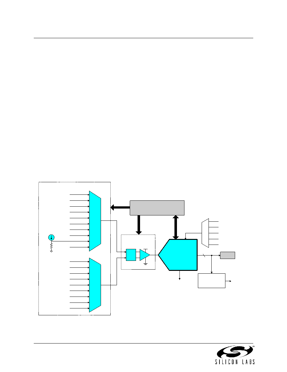
1.7.
8-Bit Analog to Digital Converter (C8051F300/2 Only)
The C8051F300/2 includes an on-chip 8-bit SAR ADC with a 10-channel differential input multiplexer and
programmable gain amplifier. With a maximum throughput of 500 ksps, the ADC offers true 8-bit accuracy
with an INL of ±1LSB. The ADC system includes a configurable analog multiplexer that selects both posi-
tive and negative ADC inputs. Each Port pin is available as an ADC input; additionally, the on-chip Temper-
ature Sensor output and the power supply voltage (VDD) are available as ADC inputs. User firmware may
shut down the ADC to save power.
The integrated programmable gain amplifier (PGA) amplifies the ADC input by 0.5, 1, 2, or 4 as defined by
user software. The gain stage is especially useful when different ADC input channels have widely varied
input voltage signals, or when it is necessary to "zoom in" on a signal with a large DC offset.
Conversions can be started in five ways: a software command, an overflow of Timer 0, 1, or 2, or an exter-
nal convert start signal. This flexibility allows the start of conversion to be triggered by software events, a
periodic signal (timer overflows), or external HW signals. Conversion completions are indicated by a status
bit and an interrupt (if enabled). The resulting 8-bit data word is latched into an SFR upon completion of a
conversion.
Window compare registers for the ADC data can be configured to interrupt the controller when ADC data is
either within or outside of a specified range. The ADC can monitor a key voltage continuously in back-
ground mode, but not interrupt the controller unless the converted data is within/outside the specified
range.
Figure 1.10. 8-Bit ADC Block Diagram
X
VDD
8
9-to-1
AMUX
Temp
Sensor
10-to-1
AMUX
VDD
P0.0
P0.1
P0.2
P0.3
P0.4
P0.5
P0.6
P0.7
P0.0
P0.1
P0.2
P0.3
P0.4
P0.5
P0.6
P0.7
DGND
Programmable Gain
Amplifier
Start
Conversion
Window Compare
Logic
Window
Compare
Interrupt
+
-
Configuration, Control, and Data Registers
Analog Multiplexer
T0 Overflow
TMR2 Overflow
T1 Overflow
Software Write
External
Convert Start
8-Bit
SAR
ADC
End of
Conversion
Interrupt
ADC Data
Register
相关PDF资料 |
PDF描述 |
|---|---|
| P87C51X2BA,512 | IC 80C51 MCU 128 RAM 44PLCC |
| C8051F536A-IM | IC 8051 MCU 2K FLASH 20QFN |
| VI-J10-IW | CONVERTER MOD DC/DC 5V 100W |
| VI-BVL-IX | CONVERTER MOD DC/DC 28V 75W |
| VI-BVJ-IX | CONVERTER MOD DC/DC 36V 75W |
相关代理商/技术参数 |
参数描述 |
|---|---|
| C8051F305-GS | 功能描述:8位微控制器 -MCU 2KB Flash RoHS:否 制造商:Silicon Labs 核心:8051 处理器系列:C8051F39x 数据总线宽度:8 bit 最大时钟频率:50 MHz 程序存储器大小:16 KB 数据 RAM 大小:1 KB 片上 ADC:Yes 工作电源电压:1.8 V to 3.6 V 工作温度范围:- 40 C to + 105 C 封装 / 箱体:QFN-20 安装风格:SMD/SMT |
| C8051F305-GSR | 功能描述:8位微控制器 -MCU 2KB 14Pin MCU RoHS:否 制造商:Silicon Labs 核心:8051 处理器系列:C8051F39x 数据总线宽度:8 bit 最大时钟频率:50 MHz 程序存储器大小:16 KB 数据 RAM 大小:1 KB 片上 ADC:Yes 工作电源电压:1.8 V to 3.6 V 工作温度范围:- 40 C to + 105 C 封装 / 箱体:QFN-20 安装风格:SMD/SMT |
| C8051F305R | 功能描述:8位微控制器 -MCU 303 2Kbyte RoHS:否 制造商:Silicon Labs 核心:8051 处理器系列:C8051F39x 数据总线宽度:8 bit 最大时钟频率:50 MHz 程序存储器大小:16 KB 数据 RAM 大小:1 KB 片上 ADC:Yes 工作电源电压:1.8 V to 3.6 V 工作温度范围:- 40 C to + 105 C 封装 / 箱体:QFN-20 安装风格:SMD/SMT |
| C8051F310 | 功能描述:8位微控制器 -MCU 16KB 10ADC RoHS:否 制造商:Silicon Labs 核心:8051 处理器系列:C8051F39x 数据总线宽度:8 bit 最大时钟频率:50 MHz 程序存储器大小:16 KB 数据 RAM 大小:1 KB 片上 ADC:Yes 工作电源电压:1.8 V to 3.6 V 工作温度范围:- 40 C to + 105 C 封装 / 箱体:QFN-20 安装风格:SMD/SMT |
| C8051F310_1 | 制造商:SILABS 制造商全称:SILABS 功能描述:8/16 kB ISP Flash MCU Family |
发布紧急采购,3分钟左右您将得到回复。