- 您现在的位置:买卖IC网 > PDF目录17090 > C8051F340-TB (Silicon Laboratories Inc)BOARD PROTOTYPING W/C8051F340 PDF资料下载
参数资料
| 型号: | C8051F340-TB |
| 厂商: | Silicon Laboratories Inc |
| 文件页数: | 131/276页 |
| 文件大小: | 0K |
| 描述: | BOARD PROTOTYPING W/C8051F340 |
| 应用说明: | TCP/IP Library Programmers Guide, Appl Note AN237 |
| 标准包装: | 1 |
| 类型: | MCU |
| 适用于相关产品: | C8051F340 |
| 所含物品: | 板 |
第1页第2页第3页第4页第5页第6页第7页第8页第9页第10页第11页第12页第13页第14页第15页第16页第17页第18页第19页第20页第21页第22页第23页第24页第25页第26页第27页第28页第29页第30页第31页第32页第33页第34页第35页第36页第37页第38页第39页第40页第41页第42页第43页第44页第45页第46页第47页第48页第49页第50页第51页第52页第53页第54页第55页第56页第57页第58页第59页第60页第61页第62页第63页第64页第65页第66页第67页第68页第69页第70页第71页第72页第73页第74页第75页第76页第77页第78页第79页第80页第81页第82页第83页第84页第85页第86页第87页第88页第89页第90页第91页第92页第93页第94页第95页第96页第97页第98页第99页第100页第101页第102页第103页第104页第105页第106页第107页第108页第109页第110页第111页第112页第113页第114页第115页第116页第117页第118页第119页第120页第121页第122页第123页第124页第125页第126页第127页第128页第129页第130页当前第131页第132页第133页第134页第135页第136页第137页第138页第139页第140页第141页第142页第143页第144页第145页第146页第147页第148页第149页第150页第151页第152页第153页第154页第155页第156页第157页第158页第159页第160页第161页第162页第163页第164页第165页第166页第167页第168页第169页第170页第171页第172页第173页第174页第175页第176页第177页第178页第179页第180页第181页第182页第183页第184页第185页第186页第187页第188页第189页第190页第191页第192页第193页第194页第195页第196页第197页第198页第199页第200页第201页第202页第203页第204页第205页第206页第207页第208页第209页第210页第211页第212页第213页第214页第215页第216页第217页第218页第219页第220页第221页第222页第223页第224页第225页第226页第227页第228页第229页第230页第231页第232页第233页第234页第235页第236页第237页第238页第239页第240页第241页第242页第243页第244页第245页第246页第247页第248页第249页第250页第251页第252页第253页第254页第255页第256页第257页第258页第259页第260页第261页第262页第263页第264页第265页第266页第267页第268页第269页第270页第271页第272页第273页第274页第275页第276页
C8051F340/1/2/3/4/5/6/7/8/9/A/B/C/D
216
Rev. 1.3
19.3. Configuration and Operation
UART1 provides standard asynchronous, full duplex communication. It can operate in a point-to-point
serial communications application, or as a node on a multi-processor serial interface. To operate in a
point-to-point application, where there are only two devices on the serial bus, the MCE1 bit in SMOD1
should be cleared to ‘0’. For operation as part of a multi-processor communications bus, the MCE1 and
XBE1 bits should both be set to ‘1’. In both types of applications, data is transmitted from the microcon-
troller on the TX1 pin, and received on the RX1 pin. The TX1 and RX1 pins are configured using the cross-
bar and the Port I/O registers, as detailed in Section “15. Port Input/Output” on page 142.
In typical UART communications, The transmit (TX) output of one device is connected to the receive (RX)
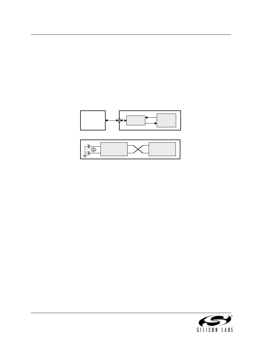
input of the other device, either directly or through a bus transceiver, as shown in Figure 19.5.
Figure 19.5. Typical UART Interconnect Diagram
19.3.1. Data Transmission
Data transmission is double-buffered, and begins when software writes a data byte to the SBUF1 register.
Writing to SBUF1 places data in the Transmit Holding Register, and the Transmit Holding Register Empty
flag (THRE1) will be cleared to ‘0’. If the UARTs shift register is empty (i.e., no transmission is in progress)
the data will be placed in the shift register, and the THRE1 bit will be set to ‘1’. If a transmission is in prog-
ress, the data will remain in the Transmit Holding Register until the current transmission is complete. The
TI1 Transmit Interrupt Flag (SCON1.1) will be set at the end of any transmission (the beginning of the
stop-bit time). If enabled, an interrupt will occur when TI1 is set.
If the extra bit function is enabled (XBE1 = ‘1’) and the parity function is disabled (PE1 = ‘0’), the value of
the TBX1 (SCON1.3) bit will be sent in the extra bit position. When the parity function is enabled (PE1 =
‘1’), hardware will generate the parity bit according to the selected parity type (selected with S1PT[1:0]),
and append it to the data field. Note: when parity is enabled, the extra bit function is not available.
19.3.2. Data Reception
Data reception can begin any time after the REN1 Receive Enable bit (SCON1.4) is set to logic 1. After the
stop bit is received, the data byte will be stored in the receive FIFO if the following conditions are met: the
receive FIFO (3 bytes deep) must not be full, and the stop bit(s) must be logic 1. In the event that the
receive FIFO is full, the incoming byte will be lost, and a Receive FIFO Overrun Error will be generated
(OVR1 in register SCON1 will be set to logic 1). If the stop bit(s) were logic 0, the incoming data will not be
stored in the receive FIFO. If the reception conditions are met, the data is stored in the receive FIFO, and
the RI1 flag will be set. Note: when MCE1 = ‘1’, RI1 will only be set if the extra bit was equal to ‘1’. Data can
be read from the receive FIFO by reading the SBUF1 register. The SBUF1 register represents the oldest
byte in the FIFO. After SBUF1 is read, the next byte in the FIFO is immediately loaded into SBUF1, and
OR
RS-232
C8051Fxxx
RS-232
LEVEL
TRANSLATOR
TX
RX
C8051Fxxx
RX
TX
MCU
RX
TX
PC
COM Port
相关PDF资料 |
PDF描述 |
|---|---|
| VE-B00-EY | CONVERTER MOD DC/DC 5V 50W |
| UVR1E682MRD6 | CAP ALUM 6800UF 25V 20% RADIAL |
| ESC10DRTS | CONN EDGECARD 20POS DIP .100 SLD |
| GBE15DHHT | CONN EDGECARD 30POS 1MM DIP SLD |
| VI-BTW-EY | CONVERTER MOD DC/DC 5.5V 50W |
相关代理商/技术参数 |
参数描述 |
|---|---|
| C8051F340-TB-K | 功能描述:BOARD PROTOTYPING W/C8051F340 制造商:silicon labs 系列:- 零件状态:在售 板类型:评估平台 类型:MCU 8-位 核心处理器:8051 操作系统:- 平台:- 配套使用产品/相关产品:C8051F340 安装类型:固定 内容:板 标准包装:1 |
| C8051F341 | 制造商:未知厂家 制造商全称:未知厂家 功能描述:Full Speed USB Flash MCU Family |
| C8051F341-GQ | 功能描述:8位微控制器 -MCU 48 MIPS 32KB 10ADC RoHS:否 制造商:Silicon Labs 核心:8051 处理器系列:C8051F39x 数据总线宽度:8 bit 最大时钟频率:50 MHz 程序存储器大小:16 KB 数据 RAM 大小:1 KB 片上 ADC:Yes 工作电源电压:1.8 V to 3.6 V 工作温度范围:- 40 C to + 105 C 封装 / 箱体:QFN-20 安装风格:SMD/SMT |
| C8051F341-GQR | 功能描述:8位微控制器 -MCU 48 MIPS 32KB 10ADC RoHS:否 制造商:Silicon Labs 核心:8051 处理器系列:C8051F39x 数据总线宽度:8 bit 最大时钟频率:50 MHz 程序存储器大小:16 KB 数据 RAM 大小:1 KB 片上 ADC:Yes 工作电源电压:1.8 V to 3.6 V 工作温度范围:- 40 C to + 105 C 封装 / 箱体:QFN-20 安装风格:SMD/SMT |
| C8051F342 | 制造商:未知厂家 制造商全称:未知厂家 功能描述:Full Speed USB Flash MCU Family |
发布紧急采购,3分钟左右您将得到回复。