- 您现在的位置:买卖IC网 > PDF目录17090 > C8051F340-TB (Silicon Laboratories Inc)BOARD PROTOTYPING W/C8051F340 PDF资料下载
参数资料
| 型号: | C8051F340-TB |
| 厂商: | Silicon Laboratories Inc |
| 文件页数: | 145/276页 |
| 文件大小: | 0K |
| 描述: | BOARD PROTOTYPING W/C8051F340 |
| 应用说明: | TCP/IP Library Programmers Guide, Appl Note AN237 |
| 标准包装: | 1 |
| 类型: | MCU |
| 适用于相关产品: | C8051F340 |
| 所含物品: | 板 |
第1页第2页第3页第4页第5页第6页第7页第8页第9页第10页第11页第12页第13页第14页第15页第16页第17页第18页第19页第20页第21页第22页第23页第24页第25页第26页第27页第28页第29页第30页第31页第32页第33页第34页第35页第36页第37页第38页第39页第40页第41页第42页第43页第44页第45页第46页第47页第48页第49页第50页第51页第52页第53页第54页第55页第56页第57页第58页第59页第60页第61页第62页第63页第64页第65页第66页第67页第68页第69页第70页第71页第72页第73页第74页第75页第76页第77页第78页第79页第80页第81页第82页第83页第84页第85页第86页第87页第88页第89页第90页第91页第92页第93页第94页第95页第96页第97页第98页第99页第100页第101页第102页第103页第104页第105页第106页第107页第108页第109页第110页第111页第112页第113页第114页第115页第116页第117页第118页第119页第120页第121页第122页第123页第124页第125页第126页第127页第128页第129页第130页第131页第132页第133页第134页第135页第136页第137页第138页第139页第140页第141页第142页第143页第144页当前第145页第146页第147页第148页第149页第150页第151页第152页第153页第154页第155页第156页第157页第158页第159页第160页第161页第162页第163页第164页第165页第166页第167页第168页第169页第170页第171页第172页第173页第174页第175页第176页第177页第178页第179页第180页第181页第182页第183页第184页第185页第186页第187页第188页第189页第190页第191页第192页第193页第194页第195页第196页第197页第198页第199页第200页第201页第202页第203页第204页第205页第206页第207页第208页第209页第210页第211页第212页第213页第214页第215页第216页第217页第218页第219页第220页第221页第222页第223页第224页第225页第226页第227页第228页第229页第230页第231页第232页第233页第234页第235页第236页第237页第238页第239页第240页第241页第242页第243页第244页第245页第246页第247页第248页第249页第250页第251页第252页第253页第254页第255页第256页第257页第258页第259页第260页第261页第262页第263页第264页第265页第266页第267页第268页第269页第270页第271页第272页第273页第274页第275页第276页
Rev. 1.3
229
C8051F340/1/2/3/4/5/6/7/8/9/A/B/C/D
20.6. SPI Special Function Registers
SPI0 is accessed and controlled through four special function registers in the system controller: SPI0CN
Control Register, SPI0DAT Data Register, SPI0CFG Configuration Register, and SPI0CKR Clock Rate
Register. The four special function registers related to the operation of the SPI0 Bus are described in the
following figures.
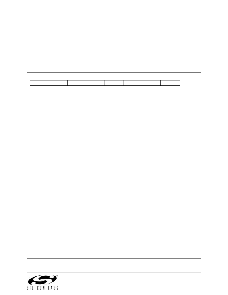
SFR Definition 20.1. SPI0CFG: SPI0 Configuration
Bit 7:
SPIBSY: SPI Busy (read only).
This bit is set to logic 1 when a SPI transfer is in progress (Master or slave Mode).
Bit 6:
MSTEN: Master Mode Enable.
0: Disable master mode. Operate in slave mode.
1: Enable master mode. Operate as a master.
Bit 5:
CKPHA: SPI0 Clock Phase.
This bit controls the SPI0 clock phase.
0: Data centered on first edge of SCK period.*
1: Data centered on second edge of SCK period.*
Bit 4:
CKPOL: SPI0 Clock Polarity.
This bit controls the SPI0 clock polarity.
0: SCK line low in idle state.
1: SCK line high in idle state.
Bit 3:
SLVSEL: Slave Selected Flag (read only).
This bit is set to logic 1 whenever the NSS pin is low indicating SPI0 is the selected slave. It
is cleared to logic 0 when NSS is high (slave not selected). This bit does not indicate the
instantaneous value at the NSS pin, but rather a de-glitched version of the pin input.
Bit 2:
NSSIN: NSS Instantaneous Pin Input (read only).
This bit mimics the instantaneous value that is present on the NSS port pin at the time that
the register is read. This input is not de-glitched.
Bit 1:
SRMT: Shift Register Empty (Valid in Slave Mode, read only).
This bit will be set to logic 1 when all data has been transferred in/out of the shift register,
and there is no new information available to read from the transmit buffer or write to the
receive buffer. It returns to logic 0 when a data byte is transferred to the shift register from
the transmit buffer or by a transition on SCK.
NOTE: SRMT = 1 when in Master Mode.
Bit 0:
RXBMT: Receive Buffer Empty (Valid in Slave Mode, read only).
This bit will be set to logic 1 when the receive buffer has been read and contains no new
information. If there is new information available in the receive buffer that has not been read,
this bit will return to logic 0.
NOTE: RXBMT = 1 when in Master Mode.
*Note: In slave mode, data on MOSI is sampled in the center of each data bit. In master mode, data on MISO is
sampled one SYSCLK before the end of each data bit, to provide maximum settling time for the slave device.
See Table 20.1 for timing parameters.
R
R/W
R
Reset Value
SPIBSY
MSTEN
CKPHA
CKPOL
SLVSEL
NSSIN
SRMT
RXBMT
00000111
Bit7
Bit6
Bit5
Bit4
Bit3
Bit2
Bit1
Bit0
SFR Address: 0xA1
相关PDF资料 |
PDF描述 |
|---|---|
| VE-B00-EY | CONVERTER MOD DC/DC 5V 50W |
| UVR1E682MRD6 | CAP ALUM 6800UF 25V 20% RADIAL |
| ESC10DRTS | CONN EDGECARD 20POS DIP .100 SLD |
| GBE15DHHT | CONN EDGECARD 30POS 1MM DIP SLD |
| VI-BTW-EY | CONVERTER MOD DC/DC 5.5V 50W |
相关代理商/技术参数 |
参数描述 |
|---|---|
| C8051F340-TB-K | 功能描述:BOARD PROTOTYPING W/C8051F340 制造商:silicon labs 系列:- 零件状态:在售 板类型:评估平台 类型:MCU 8-位 核心处理器:8051 操作系统:- 平台:- 配套使用产品/相关产品:C8051F340 安装类型:固定 内容:板 标准包装:1 |
| C8051F341 | 制造商:未知厂家 制造商全称:未知厂家 功能描述:Full Speed USB Flash MCU Family |
| C8051F341-GQ | 功能描述:8位微控制器 -MCU 48 MIPS 32KB 10ADC RoHS:否 制造商:Silicon Labs 核心:8051 处理器系列:C8051F39x 数据总线宽度:8 bit 最大时钟频率:50 MHz 程序存储器大小:16 KB 数据 RAM 大小:1 KB 片上 ADC:Yes 工作电源电压:1.8 V to 3.6 V 工作温度范围:- 40 C to + 105 C 封装 / 箱体:QFN-20 安装风格:SMD/SMT |
| C8051F341-GQR | 功能描述:8位微控制器 -MCU 48 MIPS 32KB 10ADC RoHS:否 制造商:Silicon Labs 核心:8051 处理器系列:C8051F39x 数据总线宽度:8 bit 最大时钟频率:50 MHz 程序存储器大小:16 KB 数据 RAM 大小:1 KB 片上 ADC:Yes 工作电源电压:1.8 V to 3.6 V 工作温度范围:- 40 C to + 105 C 封装 / 箱体:QFN-20 安装风格:SMD/SMT |
| C8051F342 | 制造商:未知厂家 制造商全称:未知厂家 功能描述:Full Speed USB Flash MCU Family |
发布紧急采购,3分钟左右您将得到回复。