- 您现在的位置:买卖IC网 > PDF目录3794 > C8051F366-GQ (Silicon Laboratories Inc)IC 8051 MCU 32K FLASH 32-LQFP PDF资料下载
参数资料
| 型号: | C8051F366-GQ |
| 厂商: | Silicon Laboratories Inc |
| 文件页数: | 242/288页 |
| 文件大小: | 0K |
| 描述: | IC 8051 MCU 32K FLASH 32-LQFP |
| 产品培训模块: | Serial Communication Overview |
| 标准包装: | 250 |
| 系列: | C8051F36x |
| 核心处理器: | 8051 |
| 芯体尺寸: | 8-位 |
| 速度: | 50MHz |
| 连通性: | SMBus(2 线/I²C),SPI,UART/USART |
| 外围设备: | POR,PWM,温度传感器,WDT |
| 输入/输出数: | 29 |
| 程序存储器容量: | 32KB(32K x 8) |
| 程序存储器类型: | 闪存 |
| RAM 容量: | 1K x 8 |
| 电压 - 电源 (Vcc/Vdd): | 2.7 V ~ 3.6 V |
| 数据转换器: | A/D 21x10b; D/A 1x10b |
| 振荡器型: | 内部 |
| 工作温度: | -40°C ~ 85°C |
| 封装/外壳: | 32-LQFP |
| 包装: | 托盘 |
| 配用: | 336-1410-ND - KIT DEV FOR C8051F360 FAMILY |
| 其它名称: | 336-1648 |
第1页第2页第3页第4页第5页第6页第7页第8页第9页第10页第11页第12页第13页第14页第15页第16页第17页第18页第19页第20页第21页第22页第23页第24页第25页第26页第27页第28页第29页第30页第31页第32页第33页第34页第35页第36页第37页第38页第39页第40页第41页第42页第43页第44页第45页第46页第47页第48页第49页第50页第51页第52页第53页第54页第55页第56页第57页第58页第59页第60页第61页第62页第63页第64页第65页第66页第67页第68页第69页第70页第71页第72页第73页第74页第75页第76页第77页第78页第79页第80页第81页第82页第83页第84页第85页第86页第87页第88页第89页第90页第91页第92页第93页第94页第95页第96页第97页第98页第99页第100页第101页第102页第103页第104页第105页第106页第107页第108页第109页第110页第111页第112页第113页第114页第115页第116页第117页第118页第119页第120页第121页第122页第123页第124页第125页第126页第127页第128页第129页第130页第131页第132页第133页第134页第135页第136页第137页第138页第139页第140页第141页第142页第143页第144页第145页第146页第147页第148页第149页第150页第151页第152页第153页第154页第155页第156页第157页第158页第159页第160页第161页第162页第163页第164页第165页第166页第167页第168页第169页第170页第171页第172页第173页第174页第175页第176页第177页第178页第179页第180页第181页第182页第183页第184页第185页第186页第187页第188页第189页第190页第191页第192页第193页第194页第195页第196页第197页第198页第199页第200页第201页第202页第203页第204页第205页第206页第207页第208页第209页第210页第211页第212页第213页第214页第215页第216页第217页第218页第219页第220页第221页第222页第223页第224页第225页第226页第227页第228页第229页第230页第231页第232页第233页第234页第235页第236页第237页第238页第239页第240页第241页当前第242页第243页第244页第245页第246页第247页第248页第249页第250页第251页第252页第253页第254页第255页第256页第257页第258页第259页第260页第261页第262页第263页第264页第265页第266页第267页第268页第269页第270页第271页第272页第273页第274页第275页第276页第277页第278页第279页第280页第281页第282页第283页第284页第285页第286页第287页第288页
Rev. 1.0
57
C8051F360/1/2/3/4/5/6/7/8/9
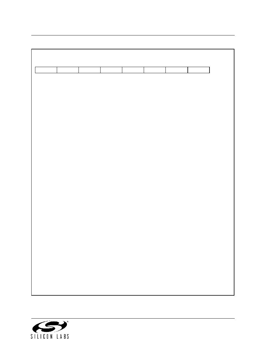
SFR Definition 5.6. ADC0CN: ADC0 Control
Bit 7:
AD0EN: ADC0 Enable Bit.
0: ADC0 Disabled. ADC0 is in low-power shutdown.
1: ADC0 Enabled. ADC0 is active and ready for data conversions.
Bit 6:
AD0TM: ADC0 Track Mode Bit.
0: Normal Track Mode: When ADC0 is enabled, tracking is continuous unless a conversion is
in progress.
1: Low-power Track Mode: Tracking Defined by AD0CM2-0 bits (see below).
Bit 5:
AD0INT: ADC0 Conversion Complete Interrupt Flag.
0: ADC0 has not completed a data conversion since the last time AD0INT was cleared.
1: ADC0 has completed a data conversion.
Bit 4:
AD0BUSY: ADC0 Busy Bit.
Read:
0: ADC0 conversion is complete or a conversion is not currently in progress. AD0INT is set to
logic ‘1’ on the falling edge of AD0BUSY.
1: ADC0 conversion is in progress.
Write:
0: No Effect.
1: Initiates ADC0 Conversion if AD0CM2-0 = 000b
Bit 3:
AD0WINT: ADC0 Window Compare Interrupt Flag.
0: ADC0 Window Comparison Data match has not occurred since this flag was last cleared.
1: ADC0 Window Comparison Data match has occurred.
Bits 2–0: AD0CM2–0: ADC0 Start of Conversion Mode Select.
When AD0TM = 0:
000: ADC0 conversion initiated on every write of ‘1’ to AD0BUSY.
001: ADC0 conversion initiated on overflow of Timer 0.
010: ADC0 conversion initiated on overflow of Timer 2.
011: ADC0 conversion initiated on overflow of Timer 1.
100: ADC0 conversion initiated on rising edge of external CNVSTR.
101: ADC0 conversion initiated on overflow of Timer 3.
11x: Reserved.
When AD0TM = 1:
000: Tracking initiated on write of ‘1’ to AD0BUSY and lasts 3 SAR clocks, followed by con-
version.
001: Tracking initiated on overflow of Timer 0 and lasts 3 SAR clocks, followed by conversion.
010: Tracking initiated on overflow of Timer 2 and lasts 3 SAR clocks, followed by conversion.
011: Tracking initiated on overflow of Timer 1 and lasts 3 SAR clocks, followed by conversion.
100: ADC0 tracks only when CNVSTR input is logic low; conversion starts on rising CNVSTR
edge.
101: Tracking initiated on overflow of Timer 3 and lasts 3 SAR clocks, followed by conversion.
11x: Reserved.
SFR Page:
SFR Address:
all pages
0xE8
(bit addressable)
R/W
Reset Value
AD0EN
AD0TM
AD0INT AD0BUSY AD0WINT AD0CM2
AD0CM1
AD0CM0 00000000
Bit7
Bit6
Bit5
Bit4
Bit3
Bit2
Bit1
Bit0
相关PDF资料 |
PDF描述 |
|---|---|
| MC68HC908QY4CDW | IC MCU 4K FLASH W/ADC 16-SOIC |
| MC68HC908QY4CP | IC MCU 4K FLASH W/ADC 16-DIP |
| MC68HC908QY2CDT | IC MCU 1.5K FLASH W/ADC 16-TSSOP |
| MC68HC908QY2CDW | IC MCU 1.5K FLASH W/ADC 16-SOIC |
| MC68HC908QY2CP | IC MCU 1.5K FLASH W/ADC 16-DIP |
相关代理商/技术参数 |
参数描述 |
|---|---|
| C8051F366-GQ1 | 制造商:SILABS 制造商全称:SILABS 功能描述:Mixed Signal ISP Flash MCU Family |
| C8051F366-GQR | 功能描述:8位微控制器 -MCU 32KB 50MIPS 10ADC 10 DAC 32Pin MCU RoHS:否 制造商:Silicon Labs 核心:8051 处理器系列:C8051F39x 数据总线宽度:8 bit 最大时钟频率:50 MHz 程序存储器大小:16 KB 数据 RAM 大小:1 KB 片上 ADC:Yes 工作电源电压:1.8 V to 3.6 V 工作温度范围:- 40 C to + 105 C 封装 / 箱体:QFN-20 安装风格:SMD/SMT |
| C8051F367 | 制造商:SILABS 制造商全称:SILABS 功能描述:Mixed Signal ISP Flash MCU Family |
| C8051F367-C-GM | 功能描述:8051 C8051F36x Microcontroller IC 8-Bit 50MHz 32KB (32K x 8) FLASH 28-QFN (5x5) 制造商:silicon labs 系列:C8051F36x 包装:管件 零件状态:Not For New Designs 核心处理器:8051 核心尺寸:8-位 速度:50MHz 连接性:SMBus(2 线/I2C),SPI,UART/USART 外设:POR,PWM,温度传感器,WDT I/O 数:25 程序存储容量:32KB(32K x 8) 程序存储器类型:闪存 EEPROM 容量:- RAM 容量:1K x 8 电压 - 电源(Vcc/Vdd):2.7 V ~ 3.6 V 数据转换器:A/D 17x10b;D/A 1x10b 振荡器类型:内部 工作温度:-40°C ~ 85°C(TA) 封装/外壳:28-VFQFN 裸露焊盘 供应商器件封装:28-QFN(5x5) 标准包装:73 |
| C8051F367-C-GMR | 功能描述:8051 C8051F36x Microcontroller IC 8-Bit 50MHz 32KB (32K x 8) FLASH 28-QFN (5x5) 制造商:silicon labs 系列:C8051F36x 包装:带卷(TR) 零件状态:Not For New Designs 核心处理器:8051 核心尺寸:8-位 速度:50MHz 连接性:SMBus(2 线/I2C),SPI,UART/USART 外设:POR,PWM,温度传感器,WDT I/O 数:25 程序存储容量:32KB(32K x 8) 程序存储器类型:闪存 EEPROM 容量:- RAM 容量:1K x 8 电压 - 电源(Vcc/Vdd):2.7 V ~ 3.6 V 数据转换器:A/D 17x10b;D/A 1x10b 振荡器类型:内部 工作温度:-40°C ~ 85°C(TA) 封装/外壳:28-VFQFN 裸露焊盘 供应商器件封装:28-QFN(5x5) 标准包装:1,500 |
发布紧急采购,3分钟左右您将得到回复。