- 您现在的位置:买卖IC网 > PDF目录3794 > C8051F366-GQ (Silicon Laboratories Inc)IC 8051 MCU 32K FLASH 32-LQFP PDF资料下载
参数资料
| 型号: | C8051F366-GQ |
| 厂商: | Silicon Laboratories Inc |
| 文件页数: | 94/288页 |
| 文件大小: | 0K |
| 描述: | IC 8051 MCU 32K FLASH 32-LQFP |
| 产品培训模块: | Serial Communication Overview |
| 标准包装: | 250 |
| 系列: | C8051F36x |
| 核心处理器: | 8051 |
| 芯体尺寸: | 8-位 |
| 速度: | 50MHz |
| 连通性: | SMBus(2 线/I²C),SPI,UART/USART |
| 外围设备: | POR,PWM,温度传感器,WDT |
| 输入/输出数: | 29 |
| 程序存储器容量: | 32KB(32K x 8) |
| 程序存储器类型: | 闪存 |
| RAM 容量: | 1K x 8 |
| 电压 - 电源 (Vcc/Vdd): | 2.7 V ~ 3.6 V |
| 数据转换器: | A/D 21x10b; D/A 1x10b |
| 振荡器型: | 内部 |
| 工作温度: | -40°C ~ 85°C |
| 封装/外壳: | 32-LQFP |
| 包装: | 托盘 |
| 配用: | 336-1410-ND - KIT DEV FOR C8051F360 FAMILY |
| 其它名称: | 336-1648 |
第1页第2页第3页第4页第5页第6页第7页第8页第9页第10页第11页第12页第13页第14页第15页第16页第17页第18页第19页第20页第21页第22页第23页第24页第25页第26页第27页第28页第29页第30页第31页第32页第33页第34页第35页第36页第37页第38页第39页第40页第41页第42页第43页第44页第45页第46页第47页第48页第49页第50页第51页第52页第53页第54页第55页第56页第57页第58页第59页第60页第61页第62页第63页第64页第65页第66页第67页第68页第69页第70页第71页第72页第73页第74页第75页第76页第77页第78页第79页第80页第81页第82页第83页第84页第85页第86页第87页第88页第89页第90页第91页第92页第93页当前第94页第95页第96页第97页第98页第99页第100页第101页第102页第103页第104页第105页第106页第107页第108页第109页第110页第111页第112页第113页第114页第115页第116页第117页第118页第119页第120页第121页第122页第123页第124页第125页第126页第127页第128页第129页第130页第131页第132页第133页第134页第135页第136页第137页第138页第139页第140页第141页第142页第143页第144页第145页第146页第147页第148页第149页第150页第151页第152页第153页第154页第155页第156页第157页第158页第159页第160页第161页第162页第163页第164页第165页第166页第167页第168页第169页第170页第171页第172页第173页第174页第175页第176页第177页第178页第179页第180页第181页第182页第183页第184页第185页第186页第187页第188页第189页第190页第191页第192页第193页第194页第195页第196页第197页第198页第199页第200页第201页第202页第203页第204页第205页第206页第207页第208页第209页第210页第211页第212页第213页第214页第215页第216页第217页第218页第219页第220页第221页第222页第223页第224页第225页第226页第227页第228页第229页第230页第231页第232页第233页第234页第235页第236页第237页第238页第239页第240页第241页第242页第243页第244页第245页第246页第247页第248页第249页第250页第251页第252页第253页第254页第255页第256页第257页第258页第259页第260页第261页第262页第263页第264页第265页第266页第267页第268页第269页第270页第271页第272页第273页第274页第275页第276页第277页第278页第279页第280页第281页第282页第283页第284页第285页第286页第287页第288页
Rev. 1.0
183
C8051F360/1/2/3/4/5/6/7/8/9
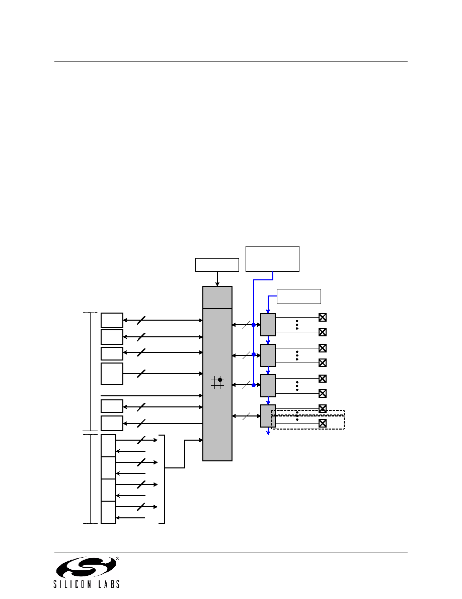
17. Port Input/Output
Digital and analog resources are available through up to 39 I/O pins. On the largest devices
(C8051F360/3), port pins are organized as four byte-wide Ports and one 7-bit-wide Port. On the other
devices (C8051F361/2/4/5/6/7/8/9), port pins are three byte-wide Ports and one partial port. Each of the
Port pins can be defined as general-purpose I/O (GPIO) or analog input/output; Port pins P0.0–P3.7 can
be assigned to one of the internal digital resources as shown in Figure 17.3. The designer has complete
control over which functions are assigned, limited only by the number of physical I/O pins. This resource
assignment flexibility is achieved through the use of a Priority Crossbar Decoder. Note that the state of a
Port I/O pin can always be read in the corresponding Port latch, regardless of the Crossbar settings.
The Crossbar assigns the selected internal digital resources to the I/O pins based on the peripheral priority
order of the Priority Decoder (Figure 17.3 and Figure 17.4). The registers XBR0 and XBR1, defined in SFR
Definition 17.1 and SFR Definition 17.2, are used to select internal digital functions.
All Port I/Os are 5 V tolerant (refer to Figure 17.2 for the Port cell circuit). The Port I/O cells are configured
as either push-pull or open-drain in the Port Output Mode registers (PnMDOUT, where n = 0,1,2,3,4). Com-
plete Electrical Specifications for Port I/O are given in Table 17.1 on page 201.
XBR0, XBR1,
PnSKIP Registers
Digital
Crossbar
Priority
Decoder
2
P0
I/O
Cells
P0.0
P0.7
8
P0MASK, P0MATCH
P1MASK, P1MATCH,
P2MASK, P2MATCH
Registers
UART
(I
nte
rna
lDi
gi
ta
lSi
gn
al
s)
Highest
Priority
Lowest
Priority
SYSCLK
2
SMBus
T0, T1
2
7
PCA
4
CP0
CP1
Outputs
SPI
4
(P
or
tLa
tc
h
es
)
P0
(P0.0-P0.7)
(P1.0-P1.7)
8
P1
P2
(P2.0-P2.7)
8
PnMDOUT,
PnMDIN Registers
3.5–3.7 available on
C8051F360/3
P3
(P3.0-P3.7)
8
P1
I/O
Cells
P1.0
P1.7
8
P2
I/O
Cell
8
P2.0
P2.7
P3
I/O
Cells
P3.0
P3.7
8
3.1–3.4 available on
C8051F360/1/3/4/6/8
Figure 17.1. Port I/O Functional Block Diagram (Port 0 through Port 3)
相关PDF资料 |
PDF描述 |
|---|---|
| MC68HC908QY4CDW | IC MCU 4K FLASH W/ADC 16-SOIC |
| MC68HC908QY4CP | IC MCU 4K FLASH W/ADC 16-DIP |
| MC68HC908QY2CDT | IC MCU 1.5K FLASH W/ADC 16-TSSOP |
| MC68HC908QY2CDW | IC MCU 1.5K FLASH W/ADC 16-SOIC |
| MC68HC908QY2CP | IC MCU 1.5K FLASH W/ADC 16-DIP |
相关代理商/技术参数 |
参数描述 |
|---|---|
| C8051F366-GQ1 | 制造商:SILABS 制造商全称:SILABS 功能描述:Mixed Signal ISP Flash MCU Family |
| C8051F366-GQR | 功能描述:8位微控制器 -MCU 32KB 50MIPS 10ADC 10 DAC 32Pin MCU RoHS:否 制造商:Silicon Labs 核心:8051 处理器系列:C8051F39x 数据总线宽度:8 bit 最大时钟频率:50 MHz 程序存储器大小:16 KB 数据 RAM 大小:1 KB 片上 ADC:Yes 工作电源电压:1.8 V to 3.6 V 工作温度范围:- 40 C to + 105 C 封装 / 箱体:QFN-20 安装风格:SMD/SMT |
| C8051F367 | 制造商:SILABS 制造商全称:SILABS 功能描述:Mixed Signal ISP Flash MCU Family |
| C8051F367-C-GM | 功能描述:8051 C8051F36x Microcontroller IC 8-Bit 50MHz 32KB (32K x 8) FLASH 28-QFN (5x5) 制造商:silicon labs 系列:C8051F36x 包装:管件 零件状态:Not For New Designs 核心处理器:8051 核心尺寸:8-位 速度:50MHz 连接性:SMBus(2 线/I2C),SPI,UART/USART 外设:POR,PWM,温度传感器,WDT I/O 数:25 程序存储容量:32KB(32K x 8) 程序存储器类型:闪存 EEPROM 容量:- RAM 容量:1K x 8 电压 - 电源(Vcc/Vdd):2.7 V ~ 3.6 V 数据转换器:A/D 17x10b;D/A 1x10b 振荡器类型:内部 工作温度:-40°C ~ 85°C(TA) 封装/外壳:28-VFQFN 裸露焊盘 供应商器件封装:28-QFN(5x5) 标准包装:73 |
| C8051F367-C-GMR | 功能描述:8051 C8051F36x Microcontroller IC 8-Bit 50MHz 32KB (32K x 8) FLASH 28-QFN (5x5) 制造商:silicon labs 系列:C8051F36x 包装:带卷(TR) 零件状态:Not For New Designs 核心处理器:8051 核心尺寸:8-位 速度:50MHz 连接性:SMBus(2 线/I2C),SPI,UART/USART 外设:POR,PWM,温度传感器,WDT I/O 数:25 程序存储容量:32KB(32K x 8) 程序存储器类型:闪存 EEPROM 容量:- RAM 容量:1K x 8 电压 - 电源(Vcc/Vdd):2.7 V ~ 3.6 V 数据转换器:A/D 17x10b;D/A 1x10b 振荡器类型:内部 工作温度:-40°C ~ 85°C(TA) 封装/外壳:28-VFQFN 裸露焊盘 供应商器件封装:28-QFN(5x5) 标准包装:1,500 |
发布紧急采购,3分钟左右您将得到回复。