- 您现在的位置:买卖IC网 > PDF目录11705 > C8051F821-GS (Silicon Laboratories Inc)IC MCU 8BIT 8KB FLASH 16SOIC PDF资料下载
参数资料
| 型号: | C8051F821-GS |
| 厂商: | Silicon Laboratories Inc |
| 文件页数: | 105/250页 |
| 文件大小: | 0K |
| 描述: | IC MCU 8BIT 8KB FLASH 16SOIC |
| 产品培训模块: | Serial Communication Overview |
| 特色产品: | QuickSense? Portfolio |
| 标准包装: | 48 |
| 系列: | C8051F82x |
| 核心处理器: | 8051 |
| 芯体尺寸: | 8-位 |
| 速度: | 25MHz |
| 连通性: | SMBus(2 线/I²C),SPI,UART/USART |
| 外围设备: | 电容感应,POR,PWM,WDT |
| 输入/输出数: | 13 |
| 程序存储器容量: | 8KB(8K x 8) |
| 程序存储器类型: | 闪存 |
| RAM 容量: | 512 x 8 |
| 电压 - 电源 (Vcc/Vdd): | 1.8 V ~ 3.6 V |
| 振荡器型: | 内部 |
| 工作温度: | -40°C ~ 85°C |
| 封装/外壳: | 16-SOIC(0.154",3.90mm 宽) |
| 包装: | 管件 |
| 产品目录页面: | 625 (CN2011-ZH PDF) |
| 其它名称: | 336-1801-5 |
第1页第2页第3页第4页第5页第6页第7页第8页第9页第10页第11页第12页第13页第14页第15页第16页第17页第18页第19页第20页第21页第22页第23页第24页第25页第26页第27页第28页第29页第30页第31页第32页第33页第34页第35页第36页第37页第38页第39页第40页第41页第42页第43页第44页第45页第46页第47页第48页第49页第50页第51页第52页第53页第54页第55页第56页第57页第58页第59页第60页第61页第62页第63页第64页第65页第66页第67页第68页第69页第70页第71页第72页第73页第74页第75页第76页第77页第78页第79页第80页第81页第82页第83页第84页第85页第86页第87页第88页第89页第90页第91页第92页第93页第94页第95页第96页第97页第98页第99页第100页第101页第102页第103页第104页当前第105页第106页第107页第108页第109页第110页第111页第112页第113页第114页第115页第116页第117页第118页第119页第120页第121页第122页第123页第124页第125页第126页第127页第128页第129页第130页第131页第132页第133页第134页第135页第136页第137页第138页第139页第140页第141页第142页第143页第144页第145页第146页第147页第148页第149页第150页第151页第152页第153页第154页第155页第156页第157页第158页第159页第160页第161页第162页第163页第164页第165页第166页第167页第168页第169页第170页第171页第172页第173页第174页第175页第176页第177页第178页第179页第180页第181页第182页第183页第184页第185页第186页第187页第188页第189页第190页第191页第192页第193页第194页第195页第196页第197页第198页第199页第200页第201页第202页第203页第204页第205页第206页第207页第208页第209页第210页第211页第212页第213页第214页第215页第216页第217页第218页第219页第220页第221页第222页第223页第224页第225页第226页第227页第228页第229页第230页第231页第232页第233页第234页第235页第236页第237页第238页第239页第240页第241页第242页第243页第244页第245页第246页第247页第248页第249页第250页
Rev. 1.0
193
C8051F80x-83x
26.5. SMBus Transfer Modes
The SMBus interface may be configured to operate as master and/or slave. At any particular time, it will be
operating in one of the following four modes: Master Transmitter, Master Receiver, Slave Transmitter, or
Slave Receiver. The SMBus interface enters Master Mode any time a START is generated, and remains in
Master Mode until it loses an arbitration or generates a STOP. An SMBus interrupt is generated at the end
of all SMBus byte frames. Note that the position of the ACK interrupt when operating as a receiver
depends on whether hardware ACK generation is enabled. As a receiver, the interrupt for an ACK occurs
before the ACK with hardware ACK generation disabled, and after the ACK when hardware ACK genera-
tion is enabled. As a transmitter, interrupts occur after the ACK, regardless of whether hardware ACK gen-
eration is enabled or not.
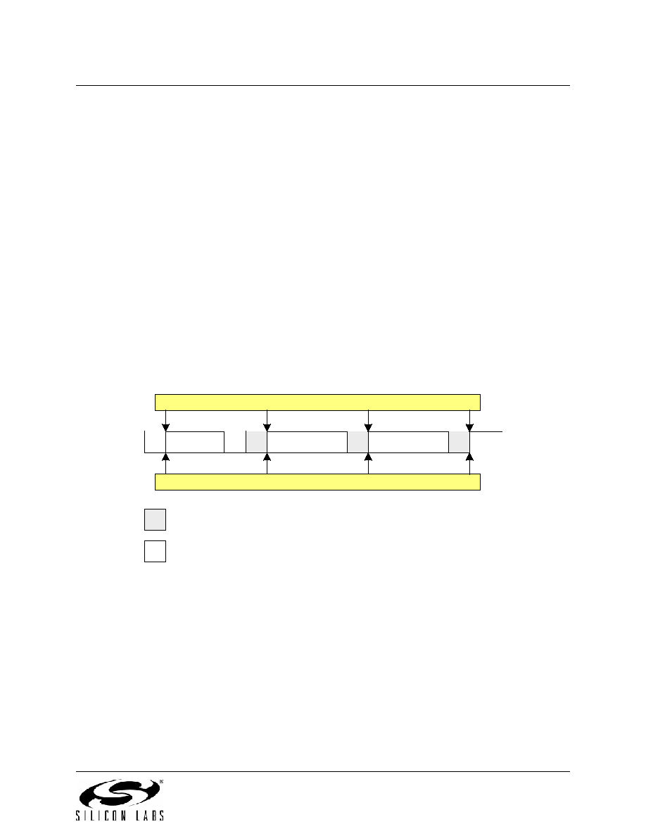
26.5.1. Write Sequence (Master)
During a write sequence, an SMBus master writes data to a slave device. The master in this transfer will be
a transmitter during the address byte, and a transmitter during all data bytes. The SMBus interface gener-
ates the START condition and transmits the first byte containing the address of the target slave and the
data direction bit. In this case the data direction bit (R/W) will be logic 0 (WRITE). The master then trans-
mits one or more bytes of serial data. After each byte is transmitted, an acknowledge bit is generated by
the slave. The transfer is ended when the STO bit is set and a STOP is generated. Note that the interface
will switch to Master Receiver Mode if SMB0DAT is not written following a Master Transmitter interrupt.
Figure 26.5 shows a typical master write sequence. Two transmit data bytes are shown, though any num-
ber of bytes may be transmitted. Notice that all of the “data byte transferred” interrupts occur after the ACK
cycle in this mode, regardless of whether hardware ACK generation is enabled.
Figure 26.5. Typical Master Write Sequence
A
S
W
P
Data Byte
SLA
S = START
P = STOP
A = ACK
W = WRITE
SLA = Slave Address
Received by SMBus
Interface
Transmitted by
SMBus Interface
Interrupts with Hardware ACK Disabled (EHACK = 0)
Interrupts with Hardware ACK Enabled (EHACK = 1)
相关PDF资料 |
PDF描述 |
|---|---|
| MS27484E22B55SA | CONN PLUG 55POS STRAIGHT W/SCKT |
| MS27484E14F35S | CONN PLUG 37POS STRAIGHT W/SCKT |
| CONSMA013.062 | CONN MALE EDGE MT FOR .062" BD |
| GTC06CF-20-15P | CONN PLUG 7POS STRAIGHT W/PINS |
| D38999/26JD18PA | CONN PLUG 18POS STRAIGHT W/PINS |
相关代理商/技术参数 |
参数描述 |
|---|---|
| C8051F821-GSR | 功能描述:8位微控制器 -MCU 8kB 512B RAM 12-CH CDC RoHS:否 制造商:Silicon Labs 核心:8051 处理器系列:C8051F39x 数据总线宽度:8 bit 最大时钟频率:50 MHz 程序存储器大小:16 KB 数据 RAM 大小:1 KB 片上 ADC:Yes 工作电源电压:1.8 V to 3.6 V 工作温度范围:- 40 C to + 105 C 封装 / 箱体:QFN-20 安装风格:SMD/SMT |
| C8051F822-GS | 功能描述:8位微控制器 -MCU 8kB, 512B RAM 8-ch CDC RoHS:否 制造商:Silicon Labs 核心:8051 处理器系列:C8051F39x 数据总线宽度:8 bit 最大时钟频率:50 MHz 程序存储器大小:16 KB 数据 RAM 大小:1 KB 片上 ADC:Yes 工作电源电压:1.8 V to 3.6 V 工作温度范围:- 40 C to + 105 C 封装 / 箱体:QFN-20 安装风格:SMD/SMT |
| C8051F822-GSR | 功能描述:8位微控制器 -MCU 8kB 512B RAM 8-CH CDC RoHS:否 制造商:Silicon Labs 核心:8051 处理器系列:C8051F39x 数据总线宽度:8 bit 最大时钟频率:50 MHz 程序存储器大小:16 KB 数据 RAM 大小:1 KB 片上 ADC:Yes 工作电源电压:1.8 V to 3.6 V 工作温度范围:- 40 C to + 105 C 封装 / 箱体:QFN-20 安装风格:SMD/SMT |
| C8051F823-GS | 功能描述:8位微控制器 -MCU 8kB, 512B RAM RoHS:否 制造商:Silicon Labs 核心:8051 处理器系列:C8051F39x 数据总线宽度:8 bit 最大时钟频率:50 MHz 程序存储器大小:16 KB 数据 RAM 大小:1 KB 片上 ADC:Yes 工作电源电压:1.8 V to 3.6 V 工作温度范围:- 40 C to + 105 C 封装 / 箱体:QFN-20 安装风格:SMD/SMT |
| C8051F823-GSR | 功能描述:8位微控制器 -MCU 8kB 512B RAM RoHS:否 制造商:Silicon Labs 核心:8051 处理器系列:C8051F39x 数据总线宽度:8 bit 最大时钟频率:50 MHz 程序存储器大小:16 KB 数据 RAM 大小:1 KB 片上 ADC:Yes 工作电源电压:1.8 V to 3.6 V 工作温度范围:- 40 C to + 105 C 封装 / 箱体:QFN-20 安装风格:SMD/SMT |
发布紧急采购,3分钟左右您将得到回复。