参数资料
| 型号: | CA3130EZ |
| 厂商: | Intersil |
| 文件页数: | 15/17页 |
| 文件大小: | 0K |
| 描述: | IC OP AMP 15MHZ BIMOS 8-DIP |
| 标准包装: | 1,000 |
| 放大器类型: | 通用 |
| 电路数: | 1 |
| 转换速率: | 30 V/µs |
| 增益带宽积: | 15MHz |
| 电流 - 输入偏压: | 5pA |
| 电压 - 输入偏移: | 8000µV |
| 电流 - 电源: | 10mA |
| 电流 - 输出 / 通道: | 45mA |
| 电压 - 电源,单路/双路(±): | 5 V ~ 16 V,±2.5 V ~ 8 V |
| 工作温度: | -55°C ~ 125°C |
| 安装类型: | 通孔 |
| 封装/外壳: | 8-DIP(0.300",7.62mm) |
| 供应商设备封装: | 8-PDIP |
| 包装: | 管件 |
7
o
Power-Supply Considerations
Because the CA3130 is very useful in single-supply
applications, it is pertinent to review some considerations
relating to power-supply current consumption under both
single-and dual-supply service. Figures 6A and 6B show the
CA3130 connected for both dual-and single-supply
operation.
Dual-supply Operation: When the output voltage at Terminal
6 is 0V, the currents supplied by the two power supplies are
equal. When the gate terminals of Q8 and Q12 are driven
increasingly positive with respect to ground, current flow
through Q12 (from the negative supply) to the load is
increased and current flow through Q8 (from the positive
supply) decreases correspondingly. When the gate terminals
of Q8 and Q12 are driven increasingly negative with respect
to ground, current flow through Q8 is increased and current
flow through Q12 is decreased accordingly.
Single-supply Operation: Initially, let it be assumed that the
value of RL is very high (or disconnected), and that the input-
terminal bias (Terminals 2 and 3) is such that the output
terminal (No. 6) voltage is at V+/2, i.e., the voltage drops
across Q8 and Q12 are of equal magnitude. Figure 20 shows
typical quiescent supply-current vs supply-voltage for the
CA3130 operated under these conditions. Since the output
stage is operating as a Class A amplifier, the supply-current
will remain constant under dynamic operating conditions as
long as the transistors are operated in the linear portion of
their voltage-transfer characteristics (see Figure 2). If either
Q8 or Q12 are swung out of their linear regions toward cut-off
(a non-linear region), there will be a corresponding reduction
in supply-current. In the extreme case, e.g., with Terminal 8
swung down to ground potential (or tied to ground), NMOS
transistor Q12 is completely cut off and the supply-current to
series-connected transistors Q8, Q12 goes essentially to zero.
The two preceding stages in the CA3130, however, continue
to draw modest supply-current (see the lower curve in Figure
20) even though the output stage is strobed off. Figure 6A
shows a dual-supply arrangement for the output stage that
can also be strobed off, assuming RL = ∞ by pulling the
potential of Terminal 8 down to that of Terminal 4.
Let it now be assumed that a load-resistance of nominal
value (e.g., 2k
) is connected between Terminal 6 and
ground in the circuit of Figure 6B. Let it be assumed again
that the input-terminal bias (Terminals 2 and 3) is such that
the output terminal (No. 6) voltage is at V+/2. Since PMOS
transistor Q8 must now supply quiescent current to both RL
and transistor Q12, it should be apparent that under these
conditions the supply-current must increase as an inverse
function of the RL magnitude. Figure 22 shows the voltage-
drop across PMOS transistor Q8 as a function of load
current at several supply voltages. Figure 2 shows the
voltage-transfer characteristics of the output stage for
several values of load resistance.
Wideband Noise
From the standpoint of low-noise performance
considerations, the use of the CA3130 is most advantageous
in applications where in the source resistance of the input
signal is on the order of 1M
or more. In this case, the total
input-referred noise voltage is typically only 23
V when the
test-circuit amplifier of Figure 7 is operated at a total supply
voltage of 15V. This value of total input-referred noise
remains essentially constant, even though the value of
source resistance is raised by an order of magnitude. This
characteristic is due to the fact that reactance of the input
capacitance becomes a significant factor in shunting the
source resistance. It should be noted, however, that for
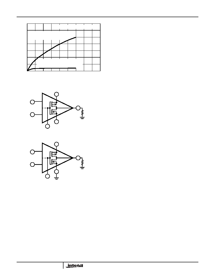
FIGURE 5. TYPICAL INCREMENTAL OFFSET-VOLTAGE
SHIFT vs OPERATING LIFE
FIGURE 6A. DUAL POWER SUPPLY OPERATION
FIGURE 6B. SINGLE POWER SUPPLY OPERATION
FIGURE 6. CA3130 OUTPUT STAGE IN DUAL AND SINGLE
POWER SUPPLY OPERATION
TA = 125
oC FOR TO-5 PACKAGES
7
6
5
4
3
2
1
0
500
1000
1500
2000 2500
3000 3500
4000
O
FFSET
V
O
L
T
A
G
E
SHI
FT
(mV)
TIME (HOURS)
DIFFERENTIAL DC VOLTAGE
(ACROSS TERMINALS 2 AND 3) = 0V
OUTPUT VOLTAGE = V+ / 2
DIFFERENTIAL DC VOLTAGE
(ACROSS TERMINALS 2 AND 3) = 2V
OUTPUT STAGE TOGGLED
0
3
2
8
4
7
6
RL
Q8
Q12
CA3130
+
-
V+
V-
3
2
8
4
7
6
RL
Q8
Q12
CA3130
+
-
V+
CA3130, CA3130A
相关PDF资料 |
PDF描述 |
|---|---|
| 68645-015 | 68645-15-CUS.HDR 2X17 |
| DIN-096CPC-SR14A-HM | CONN DIN PLUG 96POS RA GOLD |
| SZMMBZ33VALT3G | TVS ZENER 40W 33V SOT23-4 |
| 68464-240 | BERGSTIK II .100" DR STRAIGHT |
| SZMMBZ27VCLT3G | TVS ZENER 40W 27V DUAL CC SOT23 |
相关代理商/技术参数 |
参数描述 |
|---|---|
| CA3130M | 功能描述:IC OP AMP 15MHZ BIMOS 8-SOIC RoHS:否 类别:集成电路 (IC) >> Linear - Amplifiers - Instrumentation 系列:- 标准包装:1 系列:- 放大器类型:通用 电路数:4 输出类型:满摆幅 转换速率:0.6 V/µs 增益带宽积:1MHz -3db带宽:- 电流 - 输入偏压:2pA 电压 - 输入偏移:1000µV 电流 - 电源:85µA 电流 - 输出 / 通道:20mA 电压 - 电源,单路/双路(±):1.8 V ~ 6 V 工作温度:-40°C ~ 125°C 安装类型:表面贴装 封装/外壳:14-SOIC(0.154",3.90mm 宽) 供应商设备封装:14-SOICN 包装:剪切带 (CT) 产品目录页面:680 (CN2011-ZH PDF) 其它名称:MCP6L04T-E/SLCT |
| CA3130M96 | 功能描述:IC OP AMP 15MHZ BIMOS 8-SOIC RoHS:否 类别:集成电路 (IC) >> Linear - Amplifiers - Instrumentation 系列:- 标准包装:1 系列:- 放大器类型:通用 电路数:4 输出类型:满摆幅 转换速率:0.6 V/µs 增益带宽积:1MHz -3db带宽:- 电流 - 输入偏压:2pA 电压 - 输入偏移:1000µV 电流 - 电源:85µA 电流 - 输出 / 通道:20mA 电压 - 电源,单路/双路(±):1.8 V ~ 6 V 工作温度:-40°C ~ 125°C 安装类型:表面贴装 封装/外壳:14-SOIC(0.154",3.90mm 宽) 供应商设备封装:14-SOICN 包装:剪切带 (CT) 产品目录页面:680 (CN2011-ZH PDF) 其它名称:MCP6L04T-E/SLCT |
| CA3130MZ | 功能描述:运算放大器 - 运放 W/ANNEAL OPAMP 15MHZ LWBIAS 0 03NA MIL RoHS:否 制造商:STMicroelectronics 通道数量:4 共模抑制比(最小值):63 dB 输入补偿电压:1 mV 输入偏流(最大值):10 pA 工作电源电压:2.7 V to 5.5 V 安装风格:SMD/SMT 封装 / 箱体:QFN-16 转换速度:0.89 V/us 关闭:No 输出电流:55 mA 最大工作温度:+ 125 C 封装:Reel |
| CA3130MZ96 | 功能描述:运算放大器 - 运放 W/ANNEAL OPAMP 15MHZ LWBIAS 0 03NA COMP RoHS:否 制造商:STMicroelectronics 通道数量:4 共模抑制比(最小值):63 dB 输入补偿电压:1 mV 输入偏流(最大值):10 pA 工作电源电压:2.7 V to 5.5 V 安装风格:SMD/SMT 封装 / 箱体:QFN-16 转换速度:0.89 V/us 关闭:No 输出电流:55 mA 最大工作温度:+ 125 C 封装:Reel |
| CA3130S | 制造商:未知厂家 制造商全称:未知厂家 功能描述:Voltage-Feedback Operational Amplifier |
发布紧急采购,3分钟左右您将得到回复。