- 您现在的位置:买卖IC网 > PDF目录298899 > CA95C09-10CN TELECOM, DATA ENCRYPTION CIRCUIT, PQCC44 PDF资料下载
参数资料
| 型号: | CA95C09-10CN |
| 元件分类: | 加密电路 |
| 英文描述: | TELECOM, DATA ENCRYPTION CIRCUIT, PQCC44 |
| 封装: | PLASTIC, LCC-44 |
| 文件页数: | 38/42页 |
| 文件大小: | 180K |
| 代理商: | CA95C09-10CN |
第1页第2页第3页第4页第5页第6页第7页第8页第9页第10页第11页第12页第13页第14页第15页第16页第17页第18页第19页第20页第21页第22页第23页第24页第25页第26页第27页第28页第29页第30页第31页第32页第33页第34页第35页第36页第37页当前第38页第39页第40页第41页第42页
Tundra Semiconductor Corporation
CA95C68/18/09
Tundra Semiconductor Corporation
3-29
MALE
27
30
–
I
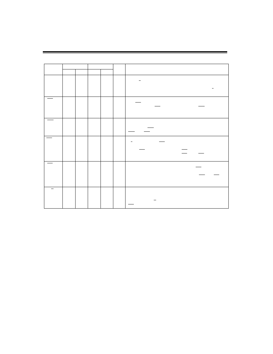
Master Port Address Latch Enable: (For CA95C68) In Multiplexed Control
Mode (C/K LOW), an active HIGH signal on this pin indicates the presence of
valid address and chip select information at the Master Port. This information
will be latched internally on the falling edge of MALE. When C/K is HIGH
(Direct Control Mode), MALE has no affect on DCP operation.
26
29
–
I
Master Port Read: (For CA95C68) This active LOW input is used with a
valid
to indicate that data is to be output on the Master Port bus.
Master Port Read (
) and Master Port Write (
) are normally
mutually exclusive; if both become active simultaneously, the DCP is reset to
ECB Mode and all ags go inactive.
28
31
–
I
Master Port Write: (For CA95C68) This active low input signal indicates to
the DCP that valid data is present on MP7-MP0 for an input operation. The
rising edge of
latches the data into the selected internal register. If
and
both go LOW simultaneously, the DCP is reset.
27
30
–
I
Master Port Address Strobe: (For CA95C18) In Multiplexed Control Mode
(C/K HIGH), a LOW on
indicates the presence of a valid chip select
signal and address information. This information will be latched on the rising
edge of
. In Direct Control Mode,
has no affect on the DCP
operation. The DCP will be reset if
and
both go low
simultaneously.
26
29
–
I
Master Port Data Strobe: (For CA95C18) This active low input is used in
conjunction with a valid Master Port Chip Select (
) to indicate that
valid data is present on the MP7-MP0 bus for an input operation or that data
is to be placed on the Master Port Bus during output.
and
are
mutually exclusive; if they both go active simultaneously, the DCP is reset to
ECB mode and all ags go inactive.
MR/W
28
31
–
I
Master Port Read/Write: (For CA95C18) This input signal indicates to the
DCP whether the current Master Port operation is a read (HIGH) where data
is transferred from the device, or a write (LOW) where data is stored to an
internal register. MR/W is not latched internally and must be held stable while
is LOW.
Table 3-2 : Pin Description Cont'd
Symbol
95C68/18
95C09
TYPE
Name and Function
PDIP
PLCC
TQFP
MRD
MCS
MRD
MWR
MRD
MAS
MDS
MCS
MDS
MAS
MDS
相关PDF资料 |
PDF描述 |
|---|---|
| CA95C09-16CN | TELECOM, DATA ENCRYPTION CIRCUIT, PQCC44 |
| CA95C09-20CN | TELECOM, DATA ENCRYPTION CIRCUIT, PQCC44 |
| CA95C09-25CN | TELECOM, DATA ENCRYPTION CIRCUIT, PQCC44 |
| CA95C09-33CN | TELECOM, DATA ENCRYPTION CIRCUIT, PQCC44 |
| CA95C09-5CN | TELECOM, DATA ENCRYPTION CIRCUIT, PQCC44 |
相关代理商/技术参数 |
参数描述 |
|---|---|
| CA96 | 制造商:Datak Corporation 功能描述: |
| CA9623-000 | 功能描述:CABLE RoHS:是 类别:线缆,导线 >> 同轴 系列:- 产品培训模块:General Cable 标准包装:1 系列:- 缆线类型:细电缆网 - 耐热阻燃型 缆线组:RG-58 线规:20 AWG(0.62mm²) 线束:19 股 / 32 AWG 套管类型:聚氯乙烯(PVC) 套管直径:0.186"(4.72mm) 屏蔽类型:箔,编织线 阻抗:50 欧姆 长度:100' (30.5m) 颜色:灰 使用:网络 特点:- 导线材料:铜,镀锡 电介质材料:多孔(泡沫)聚乙烯(多孔 FPE) 电介质直径:0.100"(2.54mm) 屏蔽材料:Flexfoil?; 铜,镀锡 屏蔽覆盖范围:100%,81% VoP,传输速度:80 工作温度:- 其它名称:C5779-100 |
| CA9652-000 | 制造商:TE Connectivity 功能描述:- Bulk |
| CA9681-000 | 制造商:TE Connectivity 功能描述:CA9681-000 |
| CA9809-000 | 制造商:TE Connectivity 功能描述:Heat Shrink Molded Boot 制造商:TE Connectivity 功能描述:222K142-25-CS-2101-0 - Bulk |
发布紧急采购,3分钟左右您将得到回复。