- 您现在的位置:买卖IC网 > PDF目录298899 > CA95C09-10CN TELECOM, DATA ENCRYPTION CIRCUIT, PQCC44 PDF资料下载
参数资料
| 型号: | CA95C09-10CN |
| 元件分类: | 加密电路 |
| 英文描述: | TELECOM, DATA ENCRYPTION CIRCUIT, PQCC44 |
| 封装: | PLASTIC, LCC-44 |
| 文件页数: | 39/42页 |
| 文件大小: | 180K |
| 代理商: | CA95C09-10CN |
第1页第2页第3页第4页第5页第6页第7页第8页第9页第10页第11页第12页第13页第14页第15页第16页第17页第18页第19页第20页第21页第22页第23页第24页第25页第26页第27页第28页第29页第30页第31页第32页第33页第34页第35页第36页第37页第38页当前第39页第40页第41页第42页
CA95C68/18/09
Tundra Semiconductor Corporation
3-30
Tundra Semiconductor Corporation
–
––29
23
I
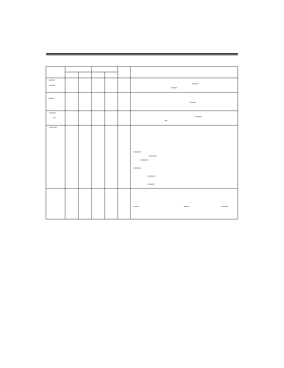
Master Port Read or Master Port Data Strobe: (For CA95C09) When the
OPTION pin is HIGH this input functions as
. When the OPTION pin is
LOW this input functions as
. (See appropriate pin description).
MALE –
_
–
30
24
I
Master Port Address Latch Enable or Master Port Address Strobe: (For
CA95C09) When the OPTION pin is HIGH this input functions as MALE and
when OPTION is LOW it functions as
. (See the appropriate pin
description).
–
MR/W
––31
25
I
Master Port Write or Master Port Read/Write: (For CA95C09) When the
OPTION pin is HIGH this input functions as
and when OPTION is
LOW it functions as MR/W. (See the appropriate pin description).
15
16
17
11
O
Master Port Flag: This active LOW ag indicates the need for a data transfer
into or out of the Master Port during normal ciphering operation. The Master
Port will be associated with either the Input or Output Register depending
upon the setting of the Control bits in the Mode Register (See Register
Description).
If data is to be transferred through the Master Port to the Input Register, then
reects the contents of the Input Register. After any Start command
is entered,
will go active (LOW) whenever the Input Register is not
full.
is forced HIGH by any command other than a Start.
Conversely, if the Master Port is associated with the Output Register,
reects the contents of the Output Register (except in single port
conguration; see Functional Description). Whenever the Output Register is
not empty
will be active (LOW). In single port mode of operation, the
Master Port ag reects the contents of the Input Register, while the Slave
Port Flag (
, see below) is associated with the Output Register.
SP7–SP0
36-39
5-2
40-43
6-3
40-43
6-3
34-37
44-41
I/O
Slave Port Bus: This 8 bit bi-directional data bus provides a second
input/output interface to the DCP, allowing overlapped input, ciphering and
output operations. The tri-state Slave Port will be accessed only when the
Mode Register is congured for dual port operation, Slave Port Chip Select
(
) and Slave Port Data Strobe (
) are both LOW and
=0.
Data entered or retrieved through this port is the most signicant byte in/out
rst (SP7 is the most signicant bit).
Table 3-2 : Pin Description Cont'd
Symbol
95C68/18
95C09
TYPE
Name and Function
PDIP
PLCC
TQFP
MRD
MDS
MRD
MDS
MAS
MWR
MFLG
SFLG
SCS
SDS
SFLG
相关PDF资料 |
PDF描述 |
|---|---|
| CA95C09-16CN | TELECOM, DATA ENCRYPTION CIRCUIT, PQCC44 |
| CA95C09-20CN | TELECOM, DATA ENCRYPTION CIRCUIT, PQCC44 |
| CA95C09-25CN | TELECOM, DATA ENCRYPTION CIRCUIT, PQCC44 |
| CA95C09-33CN | TELECOM, DATA ENCRYPTION CIRCUIT, PQCC44 |
| CA95C09-5CN | TELECOM, DATA ENCRYPTION CIRCUIT, PQCC44 |
相关代理商/技术参数 |
参数描述 |
|---|---|
| CA96 | 制造商:Datak Corporation 功能描述: |
| CA9623-000 | 功能描述:CABLE RoHS:是 类别:线缆,导线 >> 同轴 系列:- 产品培训模块:General Cable 标准包装:1 系列:- 缆线类型:细电缆网 - 耐热阻燃型 缆线组:RG-58 线规:20 AWG(0.62mm²) 线束:19 股 / 32 AWG 套管类型:聚氯乙烯(PVC) 套管直径:0.186"(4.72mm) 屏蔽类型:箔,编织线 阻抗:50 欧姆 长度:100' (30.5m) 颜色:灰 使用:网络 特点:- 导线材料:铜,镀锡 电介质材料:多孔(泡沫)聚乙烯(多孔 FPE) 电介质直径:0.100"(2.54mm) 屏蔽材料:Flexfoil?; 铜,镀锡 屏蔽覆盖范围:100%,81% VoP,传输速度:80 工作温度:- 其它名称:C5779-100 |
| CA9652-000 | 制造商:TE Connectivity 功能描述:- Bulk |
| CA9681-000 | 制造商:TE Connectivity 功能描述:CA9681-000 |
| CA9809-000 | 制造商:TE Connectivity 功能描述:Heat Shrink Molded Boot 制造商:TE Connectivity 功能描述:222K142-25-CS-2101-0 - Bulk |
发布紧急采购,3分钟左右您将得到回复。