- 您现在的位置:买卖IC网 > PDF目录16800 > CAN-OBD-RD (Silicon Laboratories Inc)KIT REF DESIGN CAN DIAGNOSTIC PDF资料下载
参数资料
| 型号: | CAN-OBD-RD |
| 厂商: | Silicon Laboratories Inc |
| 文件页数: | 88/312页 |
| 文件大小: | 0K |
| 描述: | KIT REF DESIGN CAN DIAGNOSTIC |
| 标准包装: | 1 |
| 主要目的: | 接口,CAN OBD 读取器 |
| 嵌入式: | 是,MCU,8 位 |
| 已用 IC / 零件: | C8051F502 |
| 主要属性: | CAN 板载诊断(OBD-II)参考设计 |
| 次要属性: | 支持模式 1、2 和 3,500kbps |
| 已供物品: | 板,ToolStick 适配器,线缆,CD,文档 |
| 产品目录页面: | 626 (CN2011-ZH PDF) |
| 相关产品: | 336-1515-5-ND - IC 8051 MCU 64K FLASH 32-QFN 336-1514-ND - IC 8051 MCU 64K FLASH 32-QFP |
| 其它名称: | 336-1559 |
第1页第2页第3页第4页第5页第6页第7页第8页第9页第10页第11页第12页第13页第14页第15页第16页第17页第18页第19页第20页第21页第22页第23页第24页第25页第26页第27页第28页第29页第30页第31页第32页第33页第34页第35页第36页第37页第38页第39页第40页第41页第42页第43页第44页第45页第46页第47页第48页第49页第50页第51页第52页第53页第54页第55页第56页第57页第58页第59页第60页第61页第62页第63页第64页第65页第66页第67页第68页第69页第70页第71页第72页第73页第74页第75页第76页第77页第78页第79页第80页第81页第82页第83页第84页第85页第86页第87页当前第88页第89页第90页第91页第92页第93页第94页第95页第96页第97页第98页第99页第100页第101页第102页第103页第104页第105页第106页第107页第108页第109页第110页第111页第112页第113页第114页第115页第116页第117页第118页第119页第120页第121页第122页第123页第124页第125页第126页第127页第128页第129页第130页第131页第132页第133页第134页第135页第136页第137页第138页第139页第140页第141页第142页第143页第144页第145页第146页第147页第148页第149页第150页第151页第152页第153页第154页第155页第156页第157页第158页第159页第160页第161页第162页第163页第164页第165页第166页第167页第168页第169页第170页第171页第172页第173页第174页第175页第176页第177页第178页第179页第180页第181页第182页第183页第184页第185页第186页第187页第188页第189页第190页第191页第192页第193页第194页第195页第196页第197页第198页第199页第200页第201页第202页第203页第204页第205页第206页第207页第208页第209页第210页第211页第212页第213页第214页第215页第216页第217页第218页第219页第220页第221页第222页第223页第224页第225页第226页第227页第228页第229页第230页第231页第232页第233页第234页第235页第236页第237页第238页第239页第240页第241页第242页第243页第244页第245页第246页第247页第248页第249页第250页第251页第252页第253页第254页第255页第256页第257页第258页第259页第260页第261页第262页第263页第264页第265页第266页第267页第268页第269页第270页第271页第272页第273页第274页第275页第276页第277页第278页第279页第280页第281页第282页第283页第284页第285页第286页第287页第288页第289页第290页第291页第292页第293页第294页第295页第296页第297页第298页第299页第300页第301页第302页第303页第304页第305页第306页第307页第308页第309页第310页第311页第312页
C8051F50x/F51x
178
Rev. 1.2
20.1. Port I/O Modes of Operation
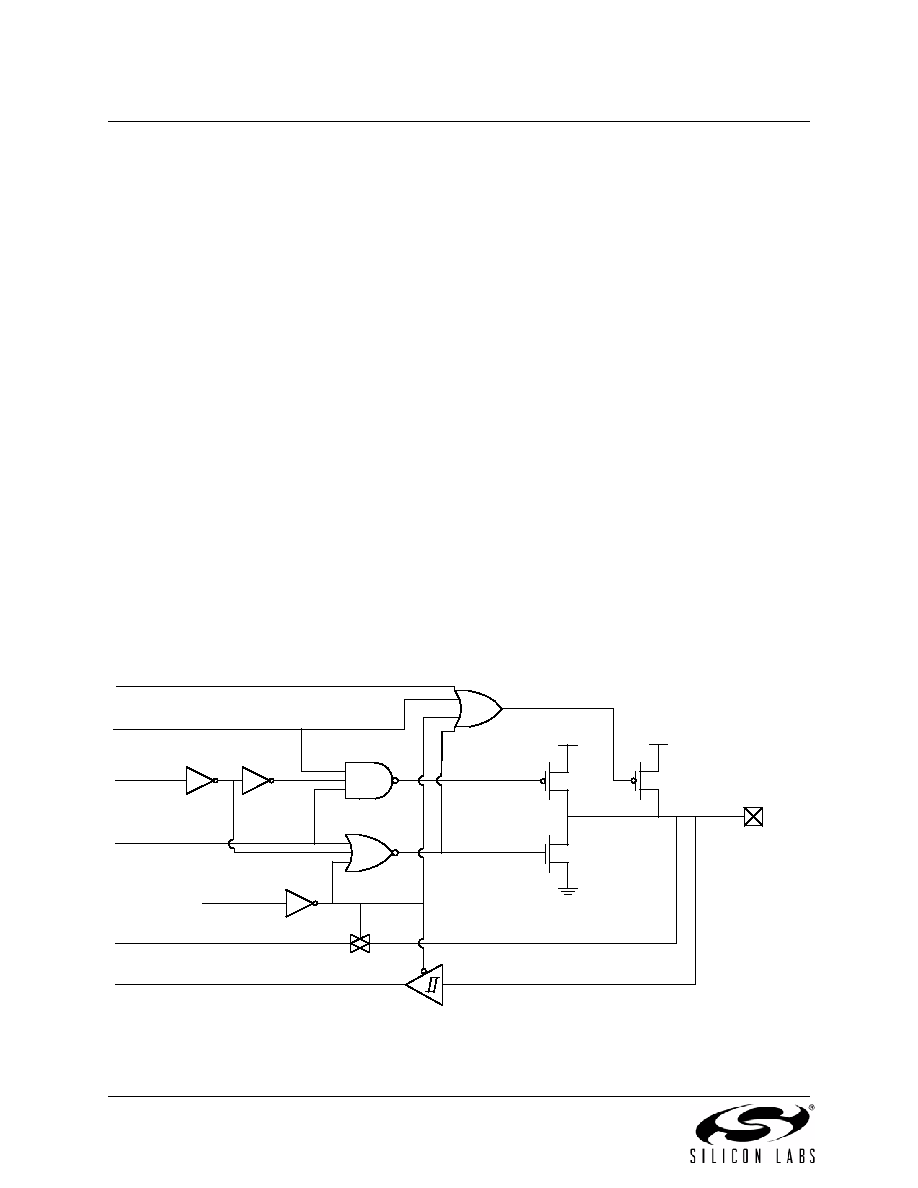
Port pins P0.0–P4.7 use the Port I/O cell shown in Figure 20.2. Each Port I/O cell can be configured by
software for analog I/O or digital I/O using the PnMDIN registers. On reset, all Port I/O cells default to a
high impedance state with weak pull-ups enabled until the Crossbar is enabled (XBARE = 1).
20.1.1. Port Pins Configured for Analog I/O
Any pins to be used as Comparator or ADC inputs, external oscillator inputs, or VREF should be config-
ured for analog I/O (PnMDIN.n = 0). When a pin is configured for analog I/O, its weak pullup, digital driver,
and digital receiver are disabled. Port pins configured for analog I/O will always read back a value of 0.
Configuring pins as analog I/O saves power and isolates the Port pin from digital interference. Port pins
configured as digital inputs may still be used by analog peripherals; however, this practice is not recom-
mended and may result in measurement errors.
20.1.2. Port Pins Configured For Digital I/O
Any pins to be used by digital peripherals (UART, SPI, SMBus, etc.), external digital event capture func-
tions, or as GPIO should be configured as digital I/O (PnMDIN.n = 1). For digital I/O pins, one of two output
modes (push-pull or open-drain) must be selected using the PnMDOUT registers.
Push-pull outputs (PnMDOUT.n = 1) drive the Port pad to the VIO or GND supply rails based on the output
logic value of the Port pin. Open-drain outputs have the high side driver disabled; therefore, they only drive
the Port pad to GND when the output logic value is 0 and become high impedance inputs (both high low
drivers turned off) when the output logic value is 1.
When a digital I/O cell is placed in the high impedance state, a weak pull-up transistor pulls the Port pad to
the VIO supply voltage to ensure the digital input is at a defined logic state. Weak pull-ups are disabled
when the I/O cell is driven to GND to minimize power consumption and may be globally disabled by setting
WEAKPUD to 1. The user should ensure that digital I/O are always internally or externally pulled or driven
to a valid logic state to minimize power consumption. Port pins configured for digital I/O always read back
the logic state of the Port pad, regardless of the output logic value of the Port pin.
Figure 20.2. Port I/O Cell Block Diagram
GND
VIO
(WEAK)
PORT
PAD
To/From Analog
Peripheral
PxMDIN.x
(1 for digital)
(0 for analog)
Px.x – Output
Logic Value
(Port Latch or
Crossbar)
XBARE
(Crossbar
Enable)
Px.x – Input Logic Value
(Reads 0 when pin is configured as an analog I/O)
PxMDOUT.x
(1 for push-pull)
(0 for open-drain)
WEAKPUD
(Weak Pull-Up Disable)
相关PDF资料 |
PDF描述 |
|---|---|
| V300C12T75BF | CONVERTER MOD DC/DC 12V 75W |
| ES1000-NO.2-B9-X-65MM | HEAT SHRINK TUBING |
| V24C24C100BL2 | CONVERTER MOD DC/DC 24V 100W |
| GBC44DCSN | CONN EDGECARD 88POS DIP .100 SLD |
| RCC18DCST-S288 | CONN EDGECARD 36POS .100 EXTEND |
相关代理商/技术参数 |
参数描述 |
|---|---|
| CANOP | 功能描述:界面模块 CAN OPTICAL REPEATER W/TB RoHS:否 制造商:B&B Electronics (Quatech) 产品: 通道/端口数量: 数据速率: 接口类型: 工作电源电压: 最大工作温度: |
| CAN-OPEN-96F340-P-P1-A | 制造商:Micrium 功能描述:UC/CAN, OPEN SENSOR SLAVE, FOR FUJITSU MB96F340, Software Application:Libraries |
| CAN-OPEN-96F340-P-P1-B | 制造商:Micrium 功能描述:UC/CAN, OPEN SENSOR SLAVE, FOR FUJITSU MB96F340, Software Application:Libraries 制造商:Micrium 功能描述:UC/CAN, OPEN SENSOR SLAVE, FOR FUJITSU MB96F340, Software Application:Libraries - CAN, Core Architecture:F2MC, Core Sub-Architecture:16FX, Supported Families:-, License Model:Product Line , RoHS Compliant: NA |
| CAN-OPEN-96F340-P-P1-C | 制造商:Micrium 功能描述:UC/CAN, OPEN SENSOR SLAVE, FOR FUJITSU MB96F340, Software Application:Libraries |
| CAN-OPEN-96F340-P-P1-PLATFORM | 制造商:Micrium 功能描述:UC/CAN OPEN SENSOR SLAVE MB96F340 制造商:Micrium 功能描述:UC/CAN, OPEN SENSOR SLAVE, MB96F340 |
发布紧急采购,3分钟左右您将得到回复。