- 您现在的位置:买卖IC网 > PDF目录169496 > CAT34WC02GYI-TE13REV-C 256 X 8 I2C/2-WIRE SERIAL EEPROM, PDSO8 PDF资料下载
参数资料
| 型号: | CAT34WC02GYI-TE13REV-C |
| 元件分类: | PROM |
| 英文描述: | 256 X 8 I2C/2-WIRE SERIAL EEPROM, PDSO8 |
| 封装: | GREEN, TSSOP-8 |
| 文件页数: | 6/10页 |
| 文件大小: | 274K |
| 代理商: | CAT34WC02GYI-TE13REV-C |
Discontinued
Part
CAT34WC02
5
Doc No. 1003, Rev. O
2005 by Catalyst Semiconductor, Inc.
Characteristics subject to change without notice
I2C BUS PROTOCOL
The following defines the features of the I2C bus proto-
col:
(1) Data transfer may be initiated only when the bus is
not busy.
(2) During a data transfer, the data line must remain
stable whenever the clock line is high. Any changes
in the data line while the clock line is high will be
interpreted as a START or STOP condition.
START Condition
The START Condition precedes all commands to the
device, and is defined as a HIGH to LOW transition of
SDA when SCL is HIGH. The CAT34WC02 monitor the
SDA and SCL lines and will not respond until this
condition is met.
STOP Condition
A LOW to HIGH transition of SDA when SCL is HIGH
determines the STOP condition. All operations must end
with a STOP condition.
DEVICE ADDRESSING
The Master begins a transmission by sending a START
condition. The Master then sends the address of the
particular slave device it is requesting. The four most
significant bits of the 8-bit slave address are fixed
(except when accessing the Write Protect Register) as
1010 for the CAT34WC02 (see Fig. 5). The next three
significant bits (A2, A1, A0) are the device address bits
and define which device the Master is accessing. Up to
eight CAT34WC02 may be individually addressed by
the system. The last bit of the slave address specifies
whether a Read or Write operation is to be performed.
When this bit is set to 1, a Read operation is selected,
and when set to 0, a Write operation is selected.
After the Master sends a START condition and the slave
address byte, the CAT34WC02 monitors the bus and
responds with an acknowledge (on the SDA line) when
its address matches the transmitted slave address. The
CAT34WC02 then performs a Read or a Write operation
depending on the state of the R/W bit.
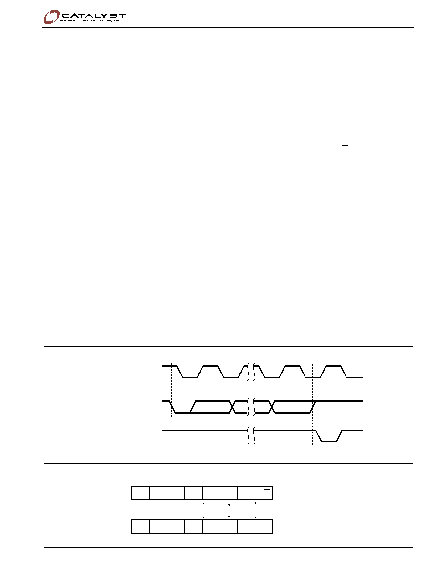
Acknowledge
After a successful data transfer, each receiving device is
required to generate an acknowledge. The Acknowledg-
ing device pulls down the SDA line during the ninth clock
cycle, signaling that it received the 8 bits of data.
The CAT34WC02 responds with an acknowledge after
receiving a START condition and its slave address. If the
device has been selected along with a write operation,
it responds with an acknowledge after receiving each
byte.
When the CAT34WC02 begins a READ mode, it trans-
mits 8 bits of data, releases the SDA line, and monitors
the line for an acknowledge. Once it receives this ac-
knowledge, the CAT34WC02 will continue to transmit
data. If no acknowledge is sent by the Master, the device
terminates data transmission and waits for a STOP
condition.
34WC02 F07
Figure 4. Acknowledge Timing
Figure 5. Slave Address Bits
5020 FHD F06
ACKNOWLEDGE
1
START
SCL FROM
MASTER
89
DATA OUTPUT
FROM TRANSMITTER
DATA OUTPUT
FROM RECEIVER
1
DEVICE ADDRESS
0
1
0
A2
A1
A0
R/W
0
1
0
A2
A1
A0
R/W
Normal Read and Write
Programming the Write
Protect Register
相关PDF资料 |
PDF描述 |
|---|---|
| CAT505J | SPECIALTY ANALOG CIRCUIT, PDSO20 |
| CAT511J-TE13 | SPECIALTY ANALOG CIRCUIT, PDSO14 |
| CAT511JI-TE13 | SPECIALTY ANALOG CIRCUIT, PDSO14 |
| CAT660CSA-TE13 | SWITCHED CAPACITOR CONVERTER, PDSO8 |
| CAT803TTBI-T10 | 1-CHANNEL POWER SUPPLY SUPPORT CKT, PDSO3 |
相关代理商/技术参数 |
参数描述 |
|---|---|
| CAT34WC02J | 功能描述:电可擦除可编程只读存储器 USE 698-CAT34WC02JI RoHS:否 制造商:Atmel 存储容量:2 Kbit 组织:256 B x 8 数据保留:100 yr 最大时钟频率:1000 KHz 最大工作电流:6 uA 工作电源电压:1.7 V to 5.5 V 最大工作温度:+ 85 C 安装风格:SMD/SMT 封装 / 箱体:SOIC-8 |
| CAT34WC02J-1.8 | 功能描述:电可擦除可编程只读存储器 (256x8) 2K 1.8-6.0 RoHS:否 制造商:Atmel 存储容量:2 Kbit 组织:256 B x 8 数据保留:100 yr 最大时钟频率:1000 KHz 最大工作电流:6 uA 工作电源电压:1.7 V to 5.5 V 最大工作温度:+ 85 C 安装风格:SMD/SMT 封装 / 箱体:SOIC-8 |
| CAT34WC02J-1.8TE13 | 制造商:CATALYST 制造商全称:Catalyst Semiconductor 功能描述:2K-Bit I2C Serial EEPROM, Serial Presence Detect |
| CAT34WC02J-2.5 | 制造商:未知厂家 制造商全称:未知厂家 功能描述:I2C Serial EEPROM |
| CAT34WC02J-2.7 | 制造商:未知厂家 制造商全称:未知厂家 功能描述:I2C Serial EEPROM |
发布紧急采购,3分钟左右您将得到回复。