- 您现在的位置:买卖IC网 > PDF目录298944 > CAT521W SPECIALTY ANALOG CIRCUIT, PDSO14 PDF资料下载
参数资料
| 型号: | CAT521W |
| 元件分类: | 模拟信号调理 |
| 英文描述: | SPECIALTY ANALOG CIRCUIT, PDSO14 |
| 封装: | LEAD-FREE, SOIC-14 |
| 文件页数: | 7/10页 |
| 文件大小: | 71K |
| 代理商: | CAT521W |
CAT521
6
Doc. No. 2003, Rev. F
As data transfers are edge triggered clean clock
transitions are necessary to avoid falsely clocking data
into the control register. Standard CMOS and TTL logic
families work well in this regard and it is recommended
that any mechanical switches used for breadboarding or
device evaluation purposes be debounced by a flip-flop
or other suitable debouncing circuit.
VREF
VREF, the voltage applied between pins VREFH &VREFL,
sets the DPP’s Zero to Full Scale output range where
VREFL = Zero and VREFH = Full Scale. VREF can span the
full power supply range or just a fraction of it. In typical
applications VREFH &VREFL are connected across the
power supply rails. When using less than the full supply
voltage be mindfull of the limits placed on VREFH and
VREFL as specified in the References section of DC
Electrical Characteristics.
READY/
BUSY
When saving data to non-volatile memory, the Ready/
Busy ouput (RDY/
BSY) signals the start and duration of
the non-volatile erase/write cycle. Upon receiving a
command to store data (PROG goes high) RDY/
BSY
goes low and remains low until the programming cycle
is complete. During this time the CAT521 will ignore any
data appearing at DI and no data will be output on DO.
RDY/
BSY is internally ANDed with a low voltage detector
circuit monitoring VDD. If VDD is below the minimum value
required for non-volatile programming, RDY/
BSY will
remain high following the program command indicating
a failure to record the desired data in non-volatile memory.
DATA OUTPUT
Data is output serially by the CAT521, LSB first, via the
Data Out (DO) pin following the reception of a start bit
and two address bits by the Data Input (DI).
DO
becomes active whenever CS goes high and resumes
its high impedance Tri-State mode when CS returns low.
Tri-Stating the DO pin allows several 521s to share a
single serial data line and simplifies interfacing multiple
521s to a microprocessor.
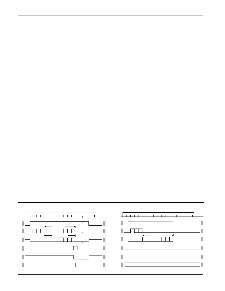
WRITING TO MEMORY
Programming the CAT521’s non-volatile memory is
accomplished through the control signals: Chip Select
(CS) and Program (PROG). With CS high, a start bit
followed by a two bit DPP address and eight data bits are
clocked into the DPP wiper control register via the DI pin.
Data enters on the clock’s rising edge. The DPP output
changes to its new setting on the clock cycle following
D7, the last data bit.
Programming is accomplished by bringing PROG high
sometime after the start bit and at least 150 ns prior to the
rising edge of the clock cycle immediately following the
D7 bit. Two clock cycles after the D7 bit the DPP wiper
control register will be ready to receive the next set of
address and data bits. The clock must be kept running
throughout the programming cycle.
Internal control
circuitry takes care of generating and ramping up the
programming voltage for data transfer to the non-volatile
memory cells. The CAT521 non-volatile memory cells
will endure over 1,000,000 write cycles and will retain
data for a minimum of 100 years without being refreshed.
READING DATA
Each time data is transferred into the DPP wiper control
register currently held data is shifted out via the D0 pin,
thus in every data transaction a read cycle occurs. Note,
however, that the reading process is destructive. Data
must be removed from the register in order to be read.
Figure 2 depicts a Read Only cycle in which no change
occurs in the DPP’s output. This feature allows
Ps to
poll DPPs for their current setting without disturbing the
output voltage but it assumes that the setting being read
is also stored in non-volatile memory so that it can be
restored at the end of the read cycle. In Figure 2 CS
returns low before the 13th clock cycle completes. In
doing so the non-volatile memory's setting is reloaded
into the DPP wiper control register. Since this value is
Figure 1. Writing to Memory
Figure 2. Reading from Memory
D0
D1
D2
D3
D4
D5
D6
D7
A0
A1
D0
D1
D2
D3
D4
D5
D6
D7
1
NEW DPP DATA
CURRENT DPP DATA
CURRENT
DPP VALUE
NON-VOLATILE
DPP
OUTPUT
PROG
DO
DI
CS
NEW
DPP VALUE
VOLATILE
NEW
DPP VALUE
NON-VOLATILE
t
1
2
3
4
5
6
7
8
9
10
11
12
N
N+1 N+2
o
RDY/BSY
A0
A1
1
DO
DI
CS
PROG
DPP
OUTPUT
t
1
2
3
4
5
6
7
8
9
10
11
12
o
CURRENT
DPP VALUE
NON-VOLATILE
D0
D1
D2
D3
D4
D5
D6
D7
CURRENT DPP DATA
RDY/BSY
相关PDF资料 |
PDF描述 |
|---|---|
| CAT706TZI-GT3 | 1-CHANNEL POWER SUPPLY MANAGEMENT CKT, PDSO8 |
| CAT813ZI-GT3 | 1-CHANNEL POWER SUPPLY MANAGEMENT CKT, PDSO8 |
| CAT809LSDI-T | 1-CHANNEL POWER SUPPLY SUPPORT CKT, PDSO3 |
| CAT809MEUR-T | 1-CHANNEL POWER SUPPLY SUPPORT CKT, PDSO3 |
| CAT809ZTBI-T | 1-CHANNEL POWER SUPPLY SUPPORT CKT, PDSO3 |
相关代理商/技术参数 |
参数描述 |
|---|---|
| CAT521WI | 功能描述:数字电位计 IC Ind Temp 28K 3-Wire RoHS:否 制造商:Maxim Integrated 电阻:200 Ohms 温度系数:35 PPM / C 容差:25 % POT 数量:Dual 每 POT 分接头:256 弧刷存储器:Volatile 缓冲刷: 数字接口:Serial (3-Wire, SPI) 描述/功能:Dual Volatile Low Voltage Linear Taper Digital Potentiometer 工作电源电压:1.7 V to 5.5 V 电源电流:27 uA 最大工作温度:+ 125 C 安装风格:SMD/SMT 封装 / 箱体:TQFN-16 封装:Reel |
| CAT521WI-T3 | 功能描述:数字电位计 IC DPP NV 256 taps 3 wire w/Buf RoHS:否 制造商:Maxim Integrated 电阻:200 Ohms 温度系数:35 PPM / C 容差:25 % POT 数量:Dual 每 POT 分接头:256 弧刷存储器:Volatile 缓冲刷: 数字接口:Serial (3-Wire, SPI) 描述/功能:Dual Volatile Low Voltage Linear Taper Digital Potentiometer 工作电源电压:1.7 V to 5.5 V 电源电流:27 uA 最大工作温度:+ 125 C 安装风格:SMD/SMT 封装 / 箱体:TQFN-16 封装:Reel |
| CAT5221WI00 | 制造商:ON Semiconductor 功能描述:DPP, NV, QUAD 64 TAPS, I2C - Rail/Tube |
| CAT5221WI-00 | 制造商:Rochester Electronics LLC 功能描述: 制造商:Catalyst Semiconductor 功能描述: |
| CAT5221WI-00-T1 | 功能描述:数字电位计 IC DPP NV QUAD 64 TAPS I2C RoHS:否 制造商:Maxim Integrated 电阻:200 Ohms 温度系数:35 PPM / C 容差:25 % POT 数量:Dual 每 POT 分接头:256 弧刷存储器:Volatile 缓冲刷: 数字接口:Serial (3-Wire, SPI) 描述/功能:Dual Volatile Low Voltage Linear Taper Digital Potentiometer 工作电源电压:1.7 V to 5.5 V 电源电流:27 uA 最大工作温度:+ 125 C 安装风格:SMD/SMT 封装 / 箱体:TQFN-16 封装:Reel |
发布紧急采购,3分钟左右您将得到回复。