- 您现在的位置:买卖IC网 > PDF目录20791 > CAT9532YI-T2 (ON Semiconductor)IC LED DRIVER LINEAR 24-TSSOP PDF资料下载
参数资料
| 型号: | CAT9532YI-T2 |
| 厂商: | ON Semiconductor |
| 文件页数: | 8/15页 |
| 文件大小: | 0K |
| 描述: | IC LED DRIVER LINEAR 24-TSSOP |
| 标准包装: | 1 |
| 拓扑: | 开路漏极,PWM |
| 输出数: | 16 |
| 内部驱动器: | 是 |
| 类型 - 主要: | 背光,LED 闪烁器 |
| 类型 - 次要: | RGB |
| 频率: | 400kHz |
| 电源电压: | 2.3 V ~ 5.5 V |
| 安装类型: | 表面贴装 |
| 封装/外壳: | 24-TSSOP(0.173",4.40mm 宽) |
| 供应商设备封装: | 24-TSSOP |
| 包装: | 标准包装 |
| 工作温度: | -40°C ~ 85°C |
| 产品目录页面: | 805 (CN2011-ZH PDF) |
| 其它名称: | CAT9532YI-T2DKR |
�� �
�
�CAT9532�
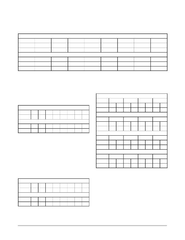
�The� Input� Register� 0� and� Input� Register� 1� reflect� the� incoming� logic� levels� of� the� I/O� pins,� regardless� of� whether� the� pin� is�
�defined� as� an� input� or� an� output.� These� registers� are� read� only� ports.� Writes� to� the� input� registers� will� be� acknowledged� but� will�
�have� no� effect.�
�Table� 7.� INPUT� REGISTER� 0� AND� INPUT� REGISTER� 1�
�INPUT0�
�LED� 7�
�LED� 6�
�LED� 5�
�LED� 4�
�LED� 3�
�LED� 2�
�LED� 1�
�LED� 0�
�bit�
�default�
�7�
�X�
�6�
�X�
�5�
�X�
�4�
�X�
�3�
�X�
�2�
�X�
�1�
�X�
�0�
�X�
�INPUT1�
�LED� 15�
�LED� 14�
�LED� 13�
�LED� 12�
�LED� 11�
�LED� 10�
�LED� 9�
�LED� 8�
�bit�
�default�
�7�
�X�
�6�
�X�
�5�
�X�
�4�
�X�
�3�
�X�
�2�
�X�
�1�
�X�
�0�
�X�
�The� Frequency� Prescaler� 0� and� Frequency� Prescaler� 1�
�registers� (PSC0,� PSC1)� are� used� to� program� the� period� of� the�
�pulse� width� modulated� signals� BLINK0� and� BLINK1�
�respectively:�
�T_BLINK0� =� (PSC0� +� 1)� /� 152;�
�T_BLINK1� =� (PSC1� +� 1)� /� 152�
�Every� LED� driver� output� can� be� programmed� to� one� of�
�four� states,� LED� OFF,� LED� ON,� LED� blinks� at� BLINK0� rate�
�and� LED� blinks� at� BLINK1� rate� using� the� LED� Selector�
�Registers� (Table� 10).�
�Table� 10.� LED� SELECTOR� REGISTERS�
�LS0�
�Table� 8.� FREQUENCY� PRESCALER� 0� AND�
�FREQUENCY� PRESCALER� 1� REGISTERS�
�PSC0�
�bit� 7� 6� 5� 4� 3� 2� 1� 0�
�default� 0� 0� 0� 0� 0� 0� 0� 0�
�PSC1�
�bit� 7� 6� 5� 4� 3� 2� 1� 0�
�default� 0� 0� 0� 0� 0� 0� 0� 0�
�The� PWM� Register� 0� and� PWM� Register� 1� (PWM0,�
�PWM1)� are� used� to� program� the� duty� cycle� of� BLINK0� and�
�BLINK1� respectively:�
�bit�
�default�
�LS1�
�bit�
�default�
�LS2�
�bit�
�LED� 3�
�7� 6�
�0� 0�
�LED� 7�
�7� 6�
�0� 0�
�LED� 11�
�7� 6�
�LED� 2�
�5� 4�
�0� 0�
�LED� 6�
�5� 4�
�0� 0�
�LED� 10�
�5� 4�
�LED� 1�
�3� 2�
�0� 0�
�LED� 5�
�3� 2�
�0� 0�
�LED� 9�
�3� 2�
�LED� 0�
�1� 0�
�0� 0�
�LED� 4�
�1� 0�
�0� 0�
�LED� 8�
�1� 0�
�Duty� Cycle_BLINK0� =� PWM0� /� 256;�
�default�
�0�
�0�
�0�
�0�
�0�
�0�
�0�
�0�
�Duty� Cycle_BLINK1� =� PWM1� /� 256�
�LS3�
�After� writing� to� the� PWM0/1� register� an� 8� ?� bit� internal�
�counter� starts� to� count� from� 0� to� 255.� The� outputs� are� low� (LED�
�on)� when� the� counter� value� is� less� than� the� value� programmed�
�into� PWM� register.� The� LED� is� off� when� the� counter� value� is�
�bit�
�default�
�LED� 15�
�7� 6�
�0� 0�
�LED� 14�
�5� 4�
�0� 0�
�LED� 13�
�3� 2�
�0� 0�
�LED� 12�
�1� 0�
�0� 0�
�higher� than� the� value� written� into� PWM� register.�
�The� LED� output� (LED0� to� LED15)� is� set� by� the� 2� bits�
�Table� 9.� PWM� REGISTER� 0� AND� PWM� REGISTER� 1�
�PWM0�
�bit� 7� 6� 5� 4� 3� 2� 1�
�0�
�value� from� the� corresponding� LSx� Register� (x� =� 0� to� 3):�
�00� =� LED� Output� set� Hi� ?� Z� (LED� Off� –� Default)�
�01� =� LED� Output� set� LOW� (LED� On)�
�10� =� LED� Output� blinks� at� BLINK0� Rate�
�default�
�1�
�0�
�0�
�0�
�0�
�0�
�0�
�0�
�11� =� LED� Output� blinks� at� BLINK1� Rate�
�PWM1�
�bit�
�default�
�7�
�1�
�6�
�0�
�5�
�0�
�4�
�0�
�3�
�0�
�2�
�0�
�1�
�0�
�0�
�0�
�http://onsemi.com�
�8�
�相关PDF资料 |
PDF描述 |
|---|---|
| GEM10DREH | CONN EDGECARD 20POS .156 EYELET |
| EBM10DTKN | CONN EDGECARD 20POS DIP .156 SLD |
| AR4PG-M3/86A | DIODE FAST REC 4A 400V SMPC |
| EBM10DTKH | CONN EDGECARD 20POS DIP .156 SLD |
| EBM10DTKD | CONN EDGECARD 20POS DIP .156 SLD |
相关代理商/技术参数 |
参数描述 |
|---|---|
| CAT9534HV4I-G | 制造商:Rochester Electronics LLC 功能描述: 制造商:Catalyst Semiconductor 功能描述: |
| CAT9534HV4I-GT2 | 功能描述:接口-I/O扩展器 8-BIT I2C/SMBUS I/O PORT RoHS:否 制造商:NXP Semiconductors 逻辑系列: 输入/输出端数量: 最大工作频率:100 kHz 工作电源电压:1.65 V to 5.5 V 工作温度范围:- 40 C to + 85 C 安装风格:SMD/SMT 封装 / 箱体:HVQFN-16 封装:Reel |
| CAT9534HV4I-GT2-CUT TAPE | 制造商:ON 功能描述:CAT9534 Series 2.3 to 5.5 V 8-bit 8 I/O I? and SMBus I/O Port - TQFN-16 |
| CAT9534WI-GT2 | 功能描述:接口-I/O扩展器 8B I2C &SMBus I/O PORT RoHS:否 制造商:NXP Semiconductors 逻辑系列: 输入/输出端数量: 最大工作频率:100 kHz 工作电源电压:1.65 V to 5.5 V 工作温度范围:- 40 C to + 85 C 安装风格:SMD/SMT 封装 / 箱体:HVQFN-16 封装:Reel |
| CAT9534YI-G | 制造商:Catalyst Semiconductor 功能描述: |
发布紧急采购,3分钟左右您将得到回复。