参数资料
| 型号: | CAV24C32WE-GT3 |
| 厂商: | ON Semiconductor |
| 文件页数: | 5/10页 |
| 文件大小: | 0K |
| 描述: | EEPROM I2C SER 32KB I2C 8SOIC |
| 标准包装: | 1 |
| 格式 - 存储器: | EEPROMs - 串行 |
| 存储器类型: | EEPROM |
| 存储容量: | 32K (4K x 8) |
| 速度: | 100kHz,400kHz |
| 接口: | I²C,2 线串口 |
| 电源电压: | 2.5 V ~ 5.5 V |
| 工作温度: | -40°C ~ 125°C |
| 封装/外壳: | 8-SOIC(0.154",3.90mm 宽) |
| 供应商设备封装: | 8-SOIC |
| 包装: | 标准包装 |
| 其它名称: | CAV24C32WE-GT3OSDKR |
�� �
�
�CAV24C32�
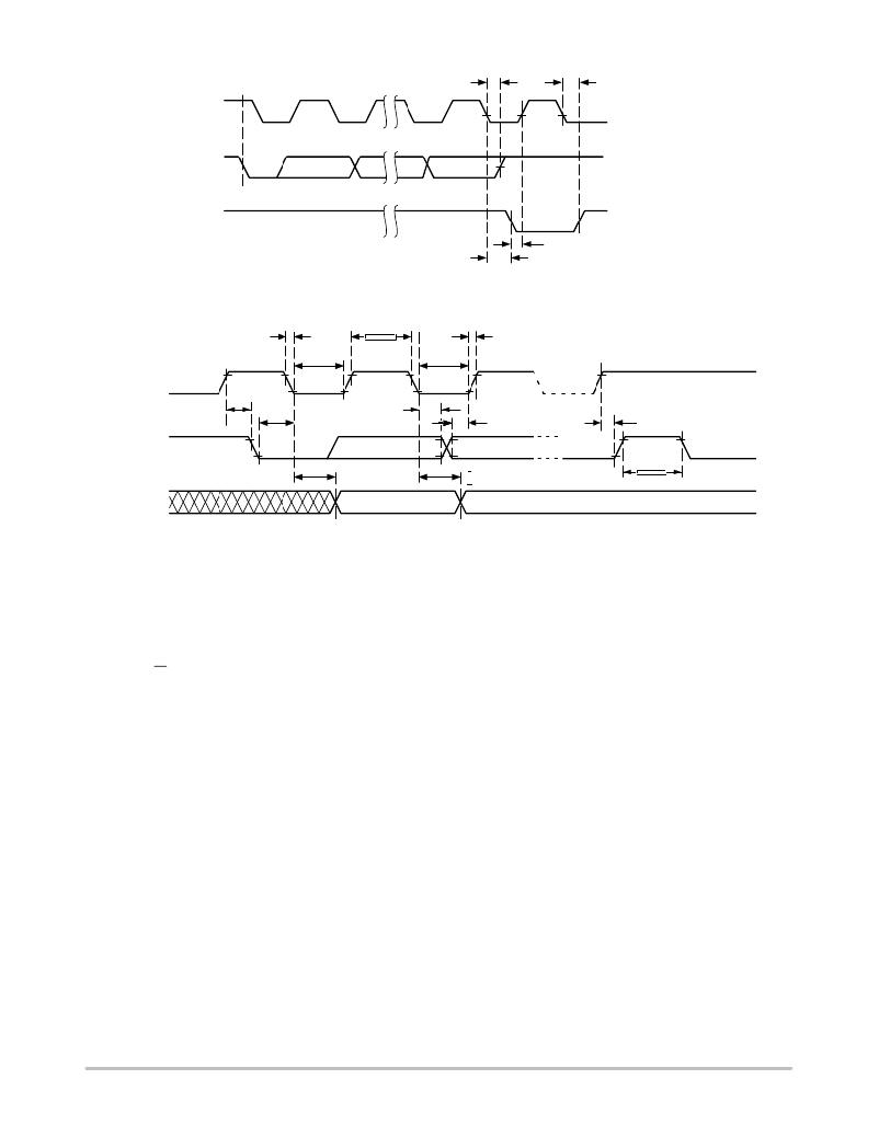
�BUS� RELEASE� DELAY� (TRANSMITTER)�
�BUS� RELEASE� DELAY� (RECEIVER)�
�SCL� FROM�
�MASTER�
�1�
�8�
�9�
�DATA� OUTPUT�
�FROM� TRANSMITTER�
�DATA� OUTPUT�
�FROM� RECEIVER�
�START�
�ACK� DELAY� (� ≤� t� AA� )�
�Figure� 4.� Acknowledge� Timing�
�ACK� SETUP� (� ≥� t� SU:DAT� )�
�SCL�
�t� F�
�t� LOW�
�t� HIGH�
�t� LOW�
�t� R�
�t� SU:STA�
�t� HD:SDA�
�t� HD:DAT�
�t� SU:DAT�
�t� SU:STO�
�SDA� IN�
�t� AA�
�t� DH�
�t� BUF�
�SDA� OUT�
�Figure� 5.� Bus� Timing�
�WRITE� OPERATIONS�
�Byte� Write�
�To� write� data� to� memory,� the� Master� creates� a� START�
�condition� on� the� bus� and� then� broadcasts� a� Slave� address�
�with� the� R/W� bit� set� to� ‘0’.� The� Master� then� sends� two�
�address� bytes� and� a� data� byte� and� concludes� the� session� by�
�creating� a� STOP� condition� on� the� bus.� The� Slave� responds�
�with� ACK� after� every� byte� sent� by� the� Master� (Figure� 6).� The�
�STOP� starts� the� internal� Write� cycle,� and� while� this�
�operation� is� in� progress� (t� WR� ),� the� SDA� output� is� tri-stated�
�and� the� Slave� does� not� acknowledge� the� Master� (Figure� 7).�
�Page� Write�
�The� Byte� Write� operation� can� be� expanded� to� Page� Write,�
�by� sending� more� than� one� data� byte� to� the� Slave� before�
�issuing� the� STOP� condition� (Figure� 8).� Up� to� 32� distinct� data�
�bytes� can� be� loaded� into� the� internal� Page� Write� Buffer�
�starting� at� the� address� provided� by� the� Master.� The� page�
�address� is� latched,� and� as� long� as� the� Master� keeps� sending�
�data,� the� internal� byte� address� is� incremented� up� to� the� end�
�of� page,� where� it� then� wraps� around� (within� the� page).� New�
�data� can� therefore� replace� data� loaded� earlier.� Following� the�
�Acknowledge� Polling�
�As� soon� (and� as� long)� as� internal� Write� is� in� progress,� the�
�Slave� will� not� acknowledge� the� Master.� This� feature� enables�
�the� Master� to� immediately� follow-up� with� a� new� Read� or�
�Write� request,� rather� than� wait� for� the� maximum� specified�
�Write� time� (t� WR� )� to� elapse.� Upon� receiving� a� NoACK�
�response� from� the� Slave,� the� Master� simply� repeats� the�
�request� until� the� Slave� responds� with� ACK.�
�Hardware� Write� Protection�
�With� the� WP� pin� held� HIGH,� the� entire� memory� is�
�protected� against� Write� operations.� If� the� WP� pin� is� left�
�floating� or� is� grounded,� it� has� no� impact� on� the� Write�
�operation.� The� state� of� the� WP� pin� is� strobed� on� the� last�
�falling� edge� of� SCL� immediately� preceding� the� 1� st� data� byte�
�(Figure� 9).� If� the� WP� pin� is� HIGH� during� the� strobe� interval,�
�the� Slave� will� not� acknowledge� the� data� byte� and� the� Write�
�request� will� be� rejected.�
�Delivery� State�
�The� CAV24C32� is� shipped� erased,� i.e.,� all� bytes� are� FFh.�
�STOP,� data� loaded� during� the� Page� Write� session� will� be�
�written� to� memory� in� a� single� internal� Write� cycle� (t� WR� ).�
�http://onsemi.com�
�5�
�相关PDF资料 |
PDF描述 |
|---|---|
| A54SX08-2VQ100I | IC FPGA SX 12K GATES 100-VQFP |
| A54SX08-2VQG100I | IC FPGA SX 12K GATES 100-VQFP |
| A54SX16-2VQG100 | IC FPGA SX 24K GATES 100-VQFP |
| A54SX16-1VQG100I | IC FPGA SX 24K GATES 100-VQFP |
| A1415A-PLG84I | IC FPGA 1500 GATES 84-PLCC |
相关代理商/技术参数 |
参数描述 |
|---|---|
| CAV24C32YE-GT3 | 功能描述:电可擦除可编程只读存储器 32KB I2C SER 电可擦除可编程只读存储器 RoHS:否 制造商:Atmel 存储容量:2 Kbit 组织:256 B x 8 数据保留:100 yr 最大时钟频率:1000 KHz 最大工作电流:6 uA 工作电源电压:1.7 V to 5.5 V 最大工作温度:+ 85 C 安装风格:SMD/SMT 封装 / 箱体:SOIC-8 |
| CAV24C512HU5EGT3 | 功能描述:IC EEPROM 512KBIT I2C 制造商:on semiconductor 系列:汽车级,AEC-Q100 零件状态:在售 存储器类型:非易失 存储器格式:EEPROM 技术:EEPROM 存储容量:512Kb (64K x 8) 时钟频率:1MHz 写周期时间 - 字,页:5ms 访问时间:400ns 存储器接口:I2C 电压 - 电源:2.5 V ~ 5.5 V 工作温度:-40°C ~ 125°C(TA) 标准包装:3,000 |
| CAV24C512WE-GT3 | 功能描述:电可擦除可编程只读存储器 512KB I2C SER 电可擦除可编程只读存储器 RoHS:否 制造商:Atmel 存储容量:2 Kbit 组织:256 B x 8 数据保留:100 yr 最大时钟频率:1000 KHz 最大工作电流:6 uA 工作电源电压:1.7 V to 5.5 V 最大工作温度:+ 85 C 安装风格:SMD/SMT 封装 / 箱体:SOIC-8 |
| CAV24C512YE-GT3 | 功能描述:电可擦除可编程只读存储器 512KB I2C SER 电可擦除可编程只读存储器 RoHS:否 制造商:Atmel 存储容量:2 Kbit 组织:256 B x 8 数据保留:100 yr 最大时钟频率:1000 KHz 最大工作电流:6 uA 工作电源电压:1.7 V to 5.5 V 最大工作温度:+ 85 C 安装风格:SMD/SMT 封装 / 箱体:SOIC-8 |
| CAV24C64 | 制造商:ONSEMI 制造商全称:ON Semiconductor 功能描述:64-Kb I2C CMOS Serial EEPROM |
发布紧急采购,3分钟左右您将得到回复。