- 您现在的位置:买卖IC网 > PDF目录26498 > CD40174BCMX (FAIRCHILD SEMICONDUCTOR CORP) PDF资料下载
参数资料
| 型号: | CD40174BCMX |
| 厂商: | FAIRCHILD SEMICONDUCTOR CORP |
| 元件分类: | 锁存器 |
| 中文描述: | 4000/14000/40000 SERIES, POSITIVE EDGE TRIGGERED D FLIP-FLOP, TRUE OUTPUT, PDSO16 |
| 封装: | 0.150 INCH, MS-012, SOIC-16 |
| 文件页数: | 3/7页 |
| 文件大小: | 68K |
| 代理商: | CD40174BCMX |
3
www.fairchildsemi.com
CD401
74BC
C
D
40
175BC
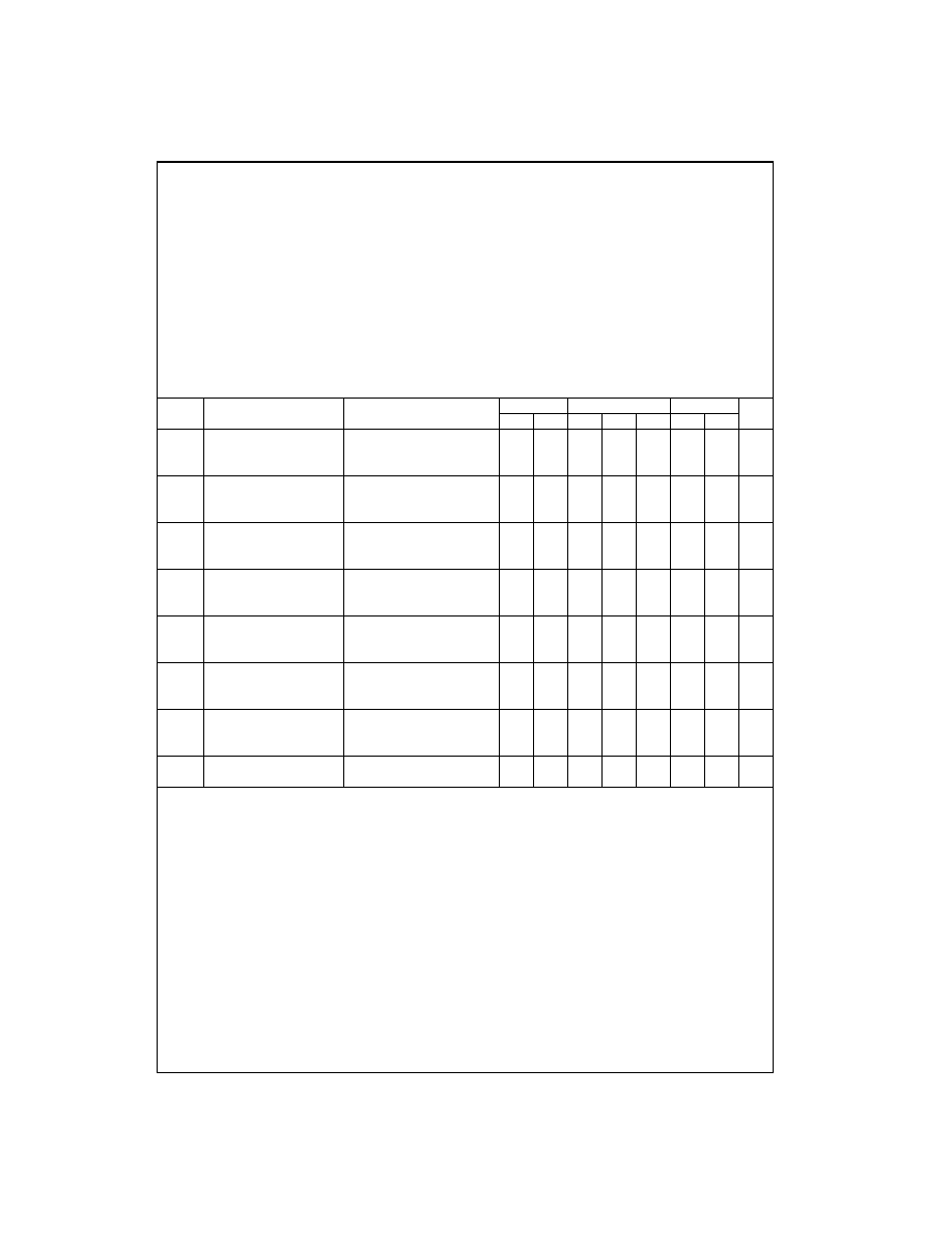
Absolute Maximum Ratings(Note 2)
(Note 3)
Recommended Operating
Conditions (Note 3)
Note 2: “Absolute Maximum Ratings” are those values beyond which the
safety of the device cannot be guaranteed. They are not meant to imply
that the devices should be operated at these limits. The tables of “Recom-
mended Operating Conditions” and “Electrical Characteristics” provide con-
ditions for actual device operation.
Note 3: VSS = 0V unless otherwise specified.
DC Electrical Characteristics (Note 3)
CD40174BC/CD40175BC
Note 4: IOH and IOL are tested one output at a time.
DC Supply Voltage (VDD)
0.5V to +18V
Input Voltage (VIN)
0.5V to V
DD +0.5 VDC
Storage Temperature Range (TS)
65°C to +150°C
Power Dissipation (PD)
Dual-In-Line
700 mW
Small Outline
500 mW
Lead Temperature (TL)
(Soldering, 10 seconds)
260
°C
DC Supply Voltage (VDD)
3V to 15 VDC
Input Voltage (VIN)
0V to VDD VDC
Operating Temperature Range (TA)
55°C to +125°C
Symbol
Parameter
Conditions
55°C
+25°C
+125°C
Units
Min
Max
Min
Typ
Max
Min
Max
IDD
Quiescent Device
VDD = 5V, VIN = VDD or VSS
1.0
30
A
Current
VDD = 10V, VIN = VDD or VSS
2.0
60
VDD = 15V, VIN = VDD or VSS
4.0
120
VOL
LOW Level Output
VDD = 5V
0.05
V
Voltage
VDD = 10V
|IO| < 1 A
0.05
VDD = 15V
0.05
VOH
HIGH Level Output
VDD = 5V
4.95
5
4.95
V
Voltage
VDD = 10V
|IO| < 1 A
9.95
10
9.95
VDD = 15V
14.95
15
14.95
VIL
LOW Level Input
VDD = 5V, VO = 0.5V or 4.5V
1.5
V
Voltage
VDD = 10V, VO = 1V or 9V
3.0
VDD = 15V, VO = 1.5V or 13.5V
4.0
VIH
HIGH Level Input
VDD = 5V, VO = 0.5V or 4.5V
3.5
V
Voltage
VDD = 10V, VO = 1V or 9V
7.0
VDD = 15V, VO = 1.5V or 13.5V
11.0
IOL
LOW Level Output
VDD = 5V, VO = 0.4V
0.64
0.51
0.88
0.36
mA
Current (Note 4)
VDD = 10V, VO = 0.5V
1.6
1.3
2.25
0.9
VDD = 15V, VO = 1.5V
4.2
3.4
8.8
2.4
IOH
HIGH Level Output
VDD = 5V, VO = 4.6V
0.64
0.51 0.88
0.36
mA
Current (Note 4)
VDD = 10V, VO = 9.5V
1.6
1.3
2.25
0.9
VDD = 15V, VO = 13.5V
4.2
3.4
8.8
2.4
IIN
Input Current
VDD = 15V, VIN = 0V
0.1
105
0.1
1.0
A
VDD = 15V, VIN = 15V
0.1
105
0.1
1.0
相关PDF资料 |
PDF描述 |
|---|---|
| CD40175BCMX | |
| CD4022BCMX | |
| CD4027BCMX | |
| CD4027BCM | |
| CD4027BCN | |
相关代理商/技术参数 |
参数描述 |
|---|---|
| CD40174BCN | 功能描述:触发器 Hex D-Type Flip-Flop RoHS:否 制造商:Texas Instruments 电路数量:2 逻辑系列:SN74 逻辑类型:D-Type Flip-Flop 极性:Inverting, Non-Inverting 输入类型:CMOS 输出类型: 传播延迟时间:4.4 ns 高电平输出电流:- 16 mA 低电平输出电流:16 mA 电源电压-最大:5.5 V 最大工作温度:+ 85 C 安装风格:SMD/SMT 封装 / 箱体:X2SON-8 封装:Reel |
| CD40174BCN/A+ | 制造商:未知厂家 制造商全称:未知厂家 功能描述:Hex D-Type Flip-Flop |
| CD40174BCN/B+ | 制造商:未知厂家 制造商全称:未知厂家 功能描述:Hex D-Type Flip-Flop |
| CD40174BD | 制造商:未知厂家 制造商全称:未知厂家 功能描述:Logic IC |
| CD40174BD3 | 制造商:Rochester Electronics LLC 功能描述:- Bulk 制造商:Harris Corporation 功能描述: |
发布紧急采购,3分钟左右您将得到回复。