参数资料
| 型号: | CD74HCT4046AMT |
| 厂商: | Texas Instruments |
| 文件页数: | 23/34页 |
| 文件大小: | 0K |
| 描述: | IC PLL W/VCO HS 16-SOIC |
| 标准包装: | 250 |
| 系列: | 74HCT |
| 类型: | 锁相环路(PLL) |
| PLL: | 是 |
| 输入: | CMOS |
| 输出: | CMOS |
| 电路数: | 1 |
| 比率 - 输入:输出: | 1:4 |
| 差分 - 输入:输出: | 无/无 |
| 频率 - 最大: | 38MHz |
| 除法器/乘法器: | 无/无 |
| 电源电压: | 4.5 V ~ 5.5 V |
| 工作温度: | -55°C ~ 125°C |
| 安装类型: | 表面贴装 |
| 封装/外壳: | 16-SOIC(0.154",3.90mm 宽) |
| 供应商设备封装: | 16-SOIC N |
| 包装: | 带卷 (TR) |
第1页第2页第3页第4页第5页第6页第7页第8页第9页第10页第11页第12页第13页第14页第15页第16页第17页第18页第19页第20页第21页第22页当前第23页第24页第25页第26页第27页第28页第29页第30页第31页第32页第33页第34页
3
General Description
VCO
The VCO requires one external capacitor C1 (between C1A
and C1B) and one external resistor R1 (between R1 and
GND) or two external resistors R1 and R2 (between R1 and
GND, and R2 and GND). Resistor R1 and capacitor C1
determine the frequency range of the VCO. Resistor R2
enables the VCO to have a frequency offset if required. See
logic diagram, Figure 1.
The high input impedance of the VCO simplies the design
of low-pass lters by giving the designer a wide choice of
resistor/capacitor ranges. In order not to load the low-pass
lter, a demodulator output of the VCO input voltage is
provided at pin 10 (DEMOUT). In contrast to conventional
techniques where the DEMOUT voltage is one threshold
voltage lower than the VCO input voltage, here the DEMOUT
voltage equals that of the VCO input. If DEMOUT is used, a
load resistor (RS) should be connected from DEMOUT to
GND; if unused, DEMOUT should be left open. The VCO
output (VCOOUT) can be connected directly to the
comparator input (COMPIN), or connected via a frequency-
divider. The VCO output signal has a specied duty factor of
50%. A LOW level at the inhibit input (INH) enables the VCO
and demodulator, while a HIGH level turns both off to
minimize standby power consumption.
Phase Comparators
The signal input (SIGIN) can be directly coupled to the self-
biasing amplier at pin 14, provided that the signal swing is
between
the
standard
HC
family
input
logic
levels.
Capacitive coupling is required for signals with smaller
swings.
Phase Comparator 1 (PC1)
This is an Exclusive-OR network. The signal and comparator
input frequencies (fi) must have a 50% duty factor to obtain
the maximum locking range. The transfer characteristic of
PC1, assuming ripple (fr = 2fi) is suppressed, is:
VDEMOUT =(VCC/π)(φSIGIN - φCOMPIN) where VDEMOUT
is the demodulator output at pin 10; VDEMOUT =VPC1OUT
(via low-pass lter).
The average output voltage from PC1, fed to the VCO input
via the low-pass lter and seen at the demodulator output at
pin 10 (VDEMOUT), is the resultant of the phase differences
of signals (SIGIN) and the comparator input (COMPIN)as
shown in Figure 2. The average of VDEM is equal to 1/2
VCC when there is no signal or noise at SIGIN, and with this
input the VCO oscillates at the center frequency (fo).
Typical waveforms for the PC1 loop locked at fo are shown
in Figure 3.
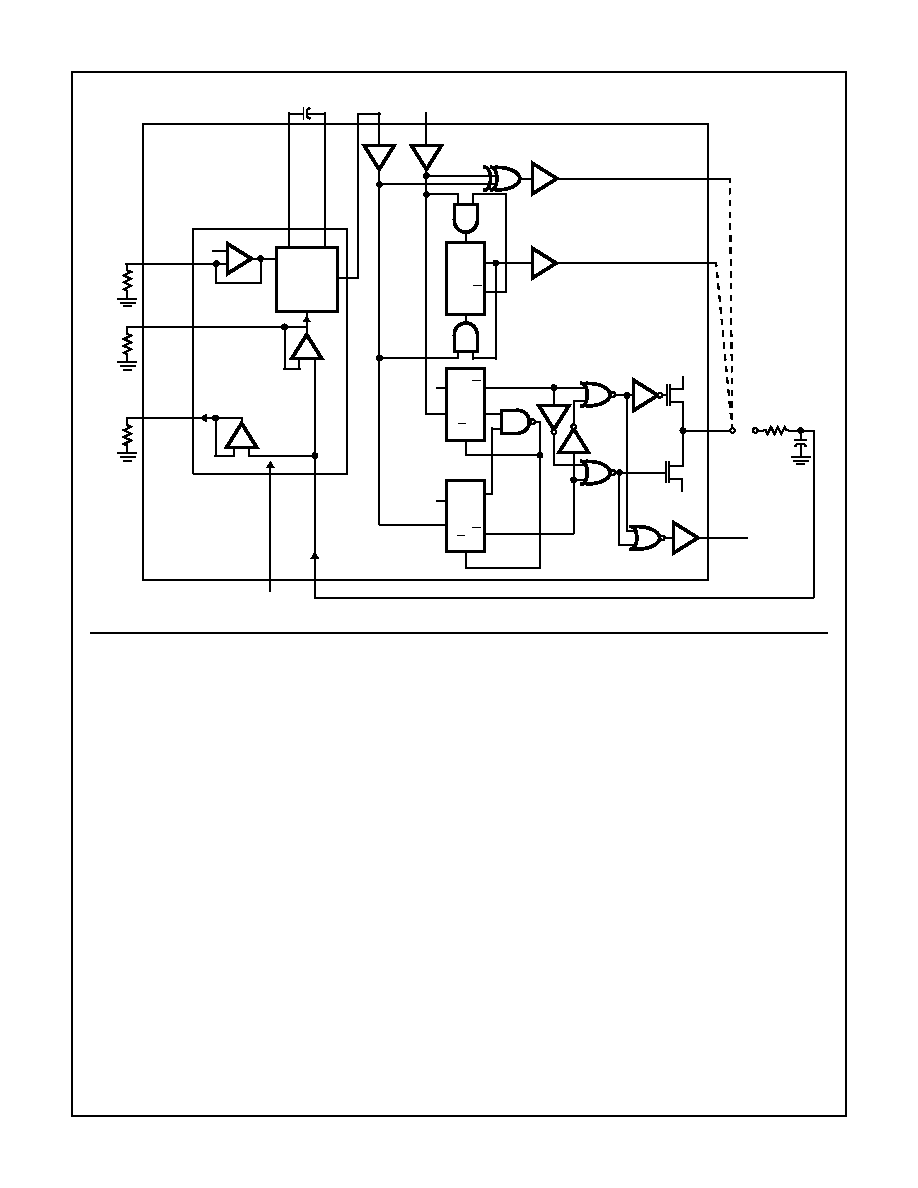
FIGURE 1. LOGIC DIAGRAM
DEMOUT
R2
12
R1
R5
11
10
C1
R3
C2
PC2OUT
13
p
n
GND
VCC
PCPOUT
1
15
2
PC3OUT
PC1OUT
DOWN
RD
Q
D
CP
RD
Q
D
CP
UP
V
CC
VCC
RD
Q
SD
INH
59
VCOIN
VCO
-
+
VCO
OUT
COMPIN
-
+
SIGIN
C1B
C1A
VREF
R2
R1
67 4
3
14
-
+
CD54HC4046A, CD74HC4046A, CD54HCT4046A, CD74HCT4046A
相关PDF资料 |
PDF描述 |
|---|---|
| V375B28H300BF2 | CONVERTER MOD DC/DC 28V 300W |
| CD74HC4046APWTE4 | IC PLL W/VCO 16-SSOP |
| V375A12T600BG3 | CONVERTER MOD DC/DC 12V 600W |
| CD74HC4046APWT | IC PLL W/VCO 16-SSOP |
| CD74HC4046APW | IC PLL W/VCO 16-TSSOP |
相关代理商/技术参数 |
参数描述 |
|---|---|
| CD74HCT4046AMTE4 | 功能描述:锁相环 - PLL Hi-Spd CMOS Logic PLL w/VCO RoHS:否 制造商:Silicon Labs 类型:PLL Clock Multiplier 电路数量:1 最大输入频率:710 MHz 最小输入频率:0.002 MHz 输出频率范围:0.002 MHz to 808 MHz 电源电压-最大:3.63 V 电源电压-最小:1.71 V 最大工作温度:+ 85 C 最小工作温度:- 40 C 封装 / 箱体:QFN-36 封装:Tray |
| CD74HCT4046AMTG4 | 功能描述:锁相环 - PLL Hi Spd CMOS Log Ph- Locked-Loop w/ VCO RoHS:否 制造商:Silicon Labs 类型:PLL Clock Multiplier 电路数量:1 最大输入频率:710 MHz 最小输入频率:0.002 MHz 输出频率范围:0.002 MHz to 808 MHz 电源电压-最大:3.63 V 电源电压-最小:1.71 V 最大工作温度:+ 85 C 最小工作温度:- 40 C 封装 / 箱体:QFN-36 封装:Tray |
| CD74HCT4051 | 制造商:HARRIS 功能描述:74HCT4051 |
| CD74HCT4051E | 功能描述:多路器开关 IC 8-Channel Analog RoHS:否 制造商:Texas Instruments 通道数量:1 开关数量:4 开启电阻(最大值):7 Ohms 开启时间(最大值): 关闭时间(最大值): 传播延迟时间:0.25 ns 工作电源电压:2.3 V to 3.6 V 工作电源电流: 最大工作温度:+ 85 C 安装风格:SMD/SMT 封装 / 箱体:UQFN-16 |
| CD74HCT4051E | 制造商:Texas Instruments 功能描述:Decoder / Encoder / Multiplexer / Demult |
发布紧急采购,3分钟左右您将得到回复。