参数资料
| 型号: | CD74HCT4046AMT |
| 厂商: | Texas Instruments |
| 文件页数: | 30/34页 |
| 文件大小: | 0K |
| 描述: | IC PLL W/VCO HS 16-SOIC |
| 标准包装: | 250 |
| 系列: | 74HCT |
| 类型: | 锁相环路(PLL) |
| PLL: | 是 |
| 输入: | CMOS |
| 输出: | CMOS |
| 电路数: | 1 |
| 比率 - 输入:输出: | 1:4 |
| 差分 - 输入:输出: | 无/无 |
| 频率 - 最大: | 38MHz |
| 除法器/乘法器: | 无/无 |
| 电源电压: | 4.5 V ~ 5.5 V |
| 工作温度: | -55°C ~ 125°C |
| 安装类型: | 表面贴装 |
| 封装/外壳: | 16-SOIC(0.154",3.90mm 宽) |
| 供应商设备封装: | 16-SOIC N |
| 包装: | 带卷 (TR) |
第1页第2页第3页第4页第5页第6页第7页第8页第9页第10页第11页第12页第13页第14页第15页第16页第17页第18页第19页第20页第21页第22页第23页第24页第25页第26页第27页第28页第29页当前第30页第31页第32页第33页第34页
5
frequency. At this stable point the voltage on C2 remains
constant as the PC2 output is in three-state and the VCO
input at pin 9 is a high impedance. Also in this condition,
the signal at the phase comparator pulse output (PCPOUT)
is a HIGH level and so can be used for indicating a locked
condition.
Thus, for PC2, no phase difference exists between SIGIN
and COMPIN over the full frequency range of the VCO.
Moreover, the power dissipation due to the low-pass lter is
reduced because both p- and n-type drivers are “OFF” for
most of the signal input cycle. It should be noted that the
PLL lock range for this type of phase comparator is equal to
the capture range and is independent of the low-pass lter.
With no signal present at SIGIN, the VCO adjusts, via PC2,
to its lowest frequency.
Phase Comparator 3 (PC3)
This
is
a
positive
edge-triggered
sequential
phase
detector using an RS-type flip-flop. When the PLL is using
this comparator, the loop is controlled by positive signal
transitions and the duty factors of SIGIN and COMPIN are
not
important.
The
transfer
characteristic
of
PC3,
assuming ripple (fr = fi) is suppressed, is:
VDEMOUT =(VCC/2p) (fSIGIN - fCOMPIN) where
VDEMOUT is the demodulator output at pin 10; VDEMOUT
= VPC3OUT (via low-pass filter).
The average output from PC3, fed to the VCO via the low-
pass filter and seen at the demodulator at pin 10
(VDEMOUT), is the resultant of the phase differences of
SIGIN and COMPIN as shown in Figure 6. Typical
waveforms for the PC3 loop locked at fo are shown in
Figure 7.
The
phase-to-output
response
characteristic
of
PC3
(Figure 6) differs from that of PC2 in that the phase angle
between SIGIN and COMPIN varies between 0
o and 360o
and is 180o at the center frequency. Also PC3 gives a
greater voltage swing than PC2 for input phase differences
but as aconsequence the ripple content of the VCO input
signal is higher. With no signal present at SIGIN, the VCO
adjusts, via PC3, to its highest frequency.
The only difference between the HC and HCT versions is the
input level specication of the INH input. This input disables
the VCO section. The comparator’s sections are identical, so
that there is no difference in the SIGIN (pin 14) or COMPIN
(pin 3) inputs between the HC and the HCT versions.
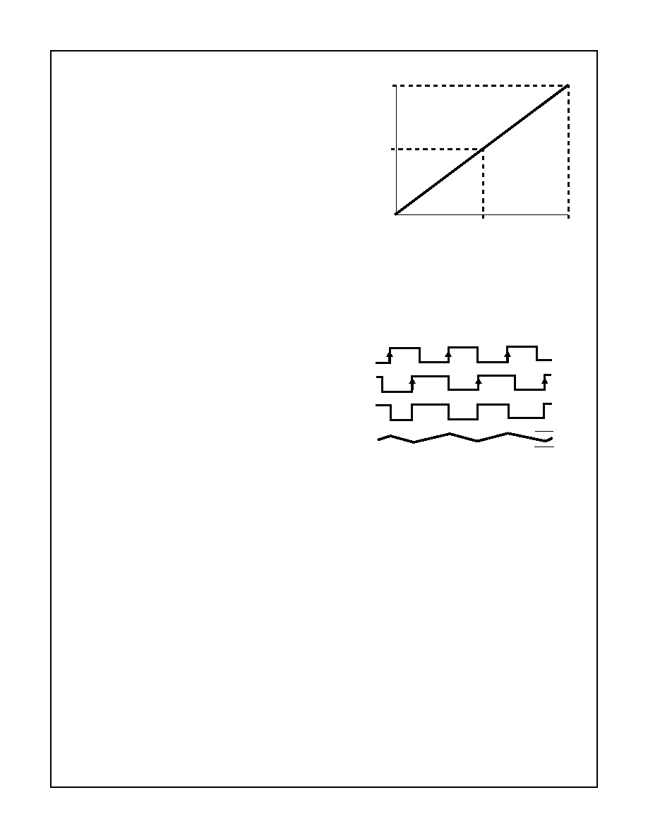
FIGURE 6. PHASE COMPARATOR 3: AVERAGE OUTPUT
VOLTAGE vs INPUT PHASE DIFFERENCE:
VDEMOUT = VPC3OUT
= (VCC/2π) (φSIGIN - φCOMPIN);
φDEMOUT = (φSIGIN - φCOMPIN)
VCC
VDEMOUT (AV)
1/2 VCC
0
0o
180o
φ
DEMOUT
360o
FIGURE 7. TYPICAL WAVEFORMS FOR PLL USING PHASE
COMPARATOR 3, LOOP LOCKED AT fo
SIGIN
COMPIN
VCOOUT
PC3OUT
VCOIN
VCC
GND
CD54HC4046A, CD74HC4046A, CD54HCT4046A, CD74HCT4046A
相关PDF资料 |
PDF描述 |
|---|---|
| V375B28H300BF2 | CONVERTER MOD DC/DC 28V 300W |
| CD74HC4046APWTE4 | IC PLL W/VCO 16-SSOP |
| V375A12T600BG3 | CONVERTER MOD DC/DC 12V 600W |
| CD74HC4046APWT | IC PLL W/VCO 16-SSOP |
| CD74HC4046APW | IC PLL W/VCO 16-TSSOP |
相关代理商/技术参数 |
参数描述 |
|---|---|
| CD74HCT4046AMTE4 | 功能描述:锁相环 - PLL Hi-Spd CMOS Logic PLL w/VCO RoHS:否 制造商:Silicon Labs 类型:PLL Clock Multiplier 电路数量:1 最大输入频率:710 MHz 最小输入频率:0.002 MHz 输出频率范围:0.002 MHz to 808 MHz 电源电压-最大:3.63 V 电源电压-最小:1.71 V 最大工作温度:+ 85 C 最小工作温度:- 40 C 封装 / 箱体:QFN-36 封装:Tray |
| CD74HCT4046AMTG4 | 功能描述:锁相环 - PLL Hi Spd CMOS Log Ph- Locked-Loop w/ VCO RoHS:否 制造商:Silicon Labs 类型:PLL Clock Multiplier 电路数量:1 最大输入频率:710 MHz 最小输入频率:0.002 MHz 输出频率范围:0.002 MHz to 808 MHz 电源电压-最大:3.63 V 电源电压-最小:1.71 V 最大工作温度:+ 85 C 最小工作温度:- 40 C 封装 / 箱体:QFN-36 封装:Tray |
| CD74HCT4051 | 制造商:HARRIS 功能描述:74HCT4051 |
| CD74HCT4051E | 功能描述:多路器开关 IC 8-Channel Analog RoHS:否 制造商:Texas Instruments 通道数量:1 开关数量:4 开启电阻(最大值):7 Ohms 开启时间(最大值): 关闭时间(最大值): 传播延迟时间:0.25 ns 工作电源电压:2.3 V to 3.6 V 工作电源电流: 最大工作温度:+ 85 C 安装风格:SMD/SMT 封装 / 箱体:UQFN-16 |
| CD74HCT4051E | 制造商:Texas Instruments 功能描述:Decoder / Encoder / Multiplexer / Demult |
发布紧急采购,3分钟左右您将得到回复。