- 您现在的位置:买卖IC网 > PDF目录378446 > CH7013A (Electronic Theatre Controls, Inc.) Digital PC to TV Encoder PDF资料下载
参数资料
| 型号: | CH7013A |
| 厂商: | Electronic Theatre Controls, Inc. |
| 英文描述: | Digital PC to TV Encoder |
| 中文描述: | 数码电脑电视编码器 |
| 文件页数: | 4/46页 |
| 文件大小: | 249K |
| 代理商: | CH7013A |
第1页第2页第3页当前第4页第5页第6页第7页第8页第9页第10页第11页第12页第13页第14页第15页第16页第17页第18页第19页第20页第21页第22页第23页第24页第25页第26页第27页第28页第29页第30页第31页第32页第33页第34页第35页第36页第37页第38页第39页第40页第41页第42页第43页第44页第45页第46页
CHRONTEL
CH7013A
4
201-0000-041 Rev. 1.0, 6/14/2000
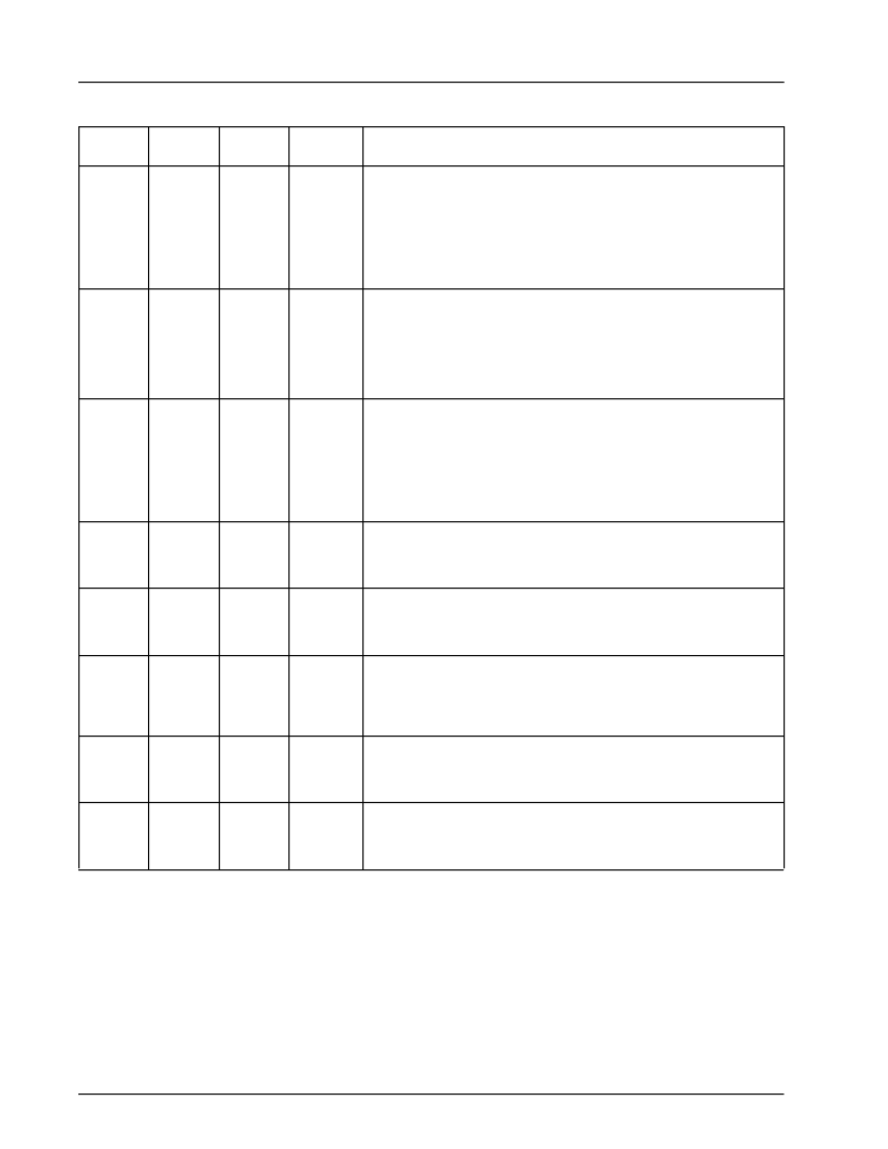
Table 1. Pin Descriptions
44-Pin
PLCC
44Pin
TQFP
Type
Symbol
Description
21-15
13-12,
10-4
15,14,
13,12,
11,10,
9,7,6,
4,3,
2,1,
44,43,42
In
D15-D0
Digital Pixel Inputs
These pins accept digital pixel data streams with either 8, 12, or 16-bit
multiplexed or 16-bit non-multiplexed formats, determined by the input
mode setting (see
Registers and Programming
section). Inputs D0 - D7
are used when operating in 8-bit multiplexed mode. Inputs D0 - D11 are
used when operating in 12-bit mode. Inputs D0 - D15 are used when
operating in 16-bit mode. The data structure and timing sequence for
each mode is described in the section on Digital Input Port.
Pixel Clock Output
The CH7013A, operating in master mode, provides a pixel data
clocking signal to the VGA controller. This pin provides the pixel clock
output signal (adjustable as X, 2X or 3X) to the VGA controller (see the
section on
Digital Video Interface
and
Registers and Programming
for
more details). The capacitive loading on this pin should be kept to a
minimum.
Pixel Clock Input
To operate in a pure master mode, the P-OUT signal should be
connected to the XCLK input pin. To operate in a pseudo-master mode,
the P-OUT clock is used as a reference frequency, and a signal locked
to this output (at 1X, 1/2X, or 1/3X the P-OUT frequency) is input to the
XCLK pin. To operate in slave mode, the CH7013A accepts an external
pixel clock input at this pin. The capacitive loading on this pin should be
kept to a minimum.
43
37
Out
P-OUT
1
39
In
XCLK
3
41
In/Out
V
Vertical Sync Input/Output
This pin accepts the vertical sync signal from the VGA controller, or
outputs a vertical sync to the VGA controller. The capacitive loading on
this pin should kept to a minimum.
Horizontal Sync Input/Output
This pin accepts the horizontal sync from the VGA controller, or outputs
a horizontal sync to the VGA controller. The capacitive loading on this
pin should be kept to a minimum.
Buffered Clock Output
This pin provides a buffered output of the 14.31818 MHz crystal input
frequency for other devices and remains active at all times (including
power-down). The output can also be selected to be other frequencies
(see
Registers and Programming
).
2
40
In/Out
H
41
35
Out
BCO
38
32
In
XI
Crystal Input
A parallel resonance 14.31818 MHz (± 50 ppm) crystal should be
attached between XI and XO/FIN. However, if an external CMOS clock
is attached to XO/FIN, XI should be connected to ground.
Crystal Output or External Fref
A 14.31818 MHz (± 50 ppm) crystal may be attached between XO/FIN
and XI. An external CMOS compatible clock can be connected to
XO/FIN as an alternative.
39
33
In
XO/FIN
相关PDF资料 |
PDF描述 |
|---|---|
| CH7013A-T | Digital PC to TV Encoder |
| CH7013A-V | Digital PC to TV Encoder |
| CHB1143 | CHB1143 |
| CHF12545CBF | 500 W Power RF Flanged Chip Termination |
| CHF12545CBF500L | 500 W Power RF Flanged Chip Termination |
相关代理商/技术参数 |
参数描述 |
|---|---|
| CH7013A-T | 制造商:未知厂家 制造商全称:未知厂家 功能描述:Digital PC to TV Encoder |
| CH7013A-V | 制造商:未知厂家 制造商全称:未知厂家 功能描述:Digital PC to TV Encoder |
| CH7013B | 制造商:未知厂家 制造商全称:未知厂家 功能描述:Digital PC to TV Encoder |
| CH7013B-D | 制造商:未知厂家 制造商全称:未知厂家 功能描述:Digital PC to TV Encoder |
| CH7013B-DF | 制造商:未知厂家 制造商全称:未知厂家 功能描述:Digital PC to TV Encoder |
发布紧急采购,3分钟左右您将得到回复。