- 您现在的位置:买卖IC网 > PDF目录11751 > CMP82C55AZ (Intersil)IC PROG PERIPHERAL INTFC 40-PDIP PDF资料下载
参数资料
| 型号: | CMP82C55AZ |
| 厂商: | Intersil |
| 文件页数: | 3/26页 |
| 文件大小: | 0K |
| 描述: | IC PROG PERIPHERAL INTFC 40-PDIP |
| 标准包装: | 99 |
| 接口: | 总线 |
| 电源电压: | 4.5 V ~ 5.5 V |
| 封装/外壳: | 40-DIP(0.600",15.24mm) |
| 供应商设备封装: | 40-DIP |
| 包装: | 管件 |
| 安装类型: | 通孔 |
11
FN6140.2
June 15, 2006
Operating Modes
Mode 2 (Strobed Bidirectional Bus I/O)
This functional configuration provides a means for
communicating with a peripheral device or structure on a
single 8-bit bus for both transmitting and receiving data
(bidirectional bus I/O). “Hand shaking” signals are provided to
maintain proper bus flow discipline similar to Mode 1. Interrupt
generation and enable/disable functions are also available.
Mode 2 Basic Functional Definitions:
Used in Group A only
One 8-bit, bidirectional bus Port (Port A) and a 5-bit
control Port (Port C)
Both inputs and outputs are latched
The 5-bit control port (Port C) is used for control and
status for the 8-bit, bidirectional bus port (Port A)
Bidirectional Bus I/O Control Signal Definition
(Figures 11, 12, 13, 14)
INTR - (Interrupt Request). A high on this output can be
used to interrupt the CPU for both input or output operations.
Output Operations
OBF - (Output Buffer Full). The OBF output will go “low” to
indicate that the CPU has written data out to port A.
ACK - (Acknowledge). A “low” on this input enables the three-
state output buffer of port A to send out the data. Otherwise,
the output buffer will be in the high impedance state.
INTE 1 - (The INTE flip-flop associated with OBF).
Controlled by bit set/reset of PC4.
Input Operations
STB - (Strobe Input). A “low” on this input loads data into the
input latch.
IBF - (Input Buffer Full F/F). A “high” on this output indicates
that data has been loaded into the input latch.
INTE 2 - (The INTE flip-flop associated with IBF). Controlled
by bit set/reset of PC4.
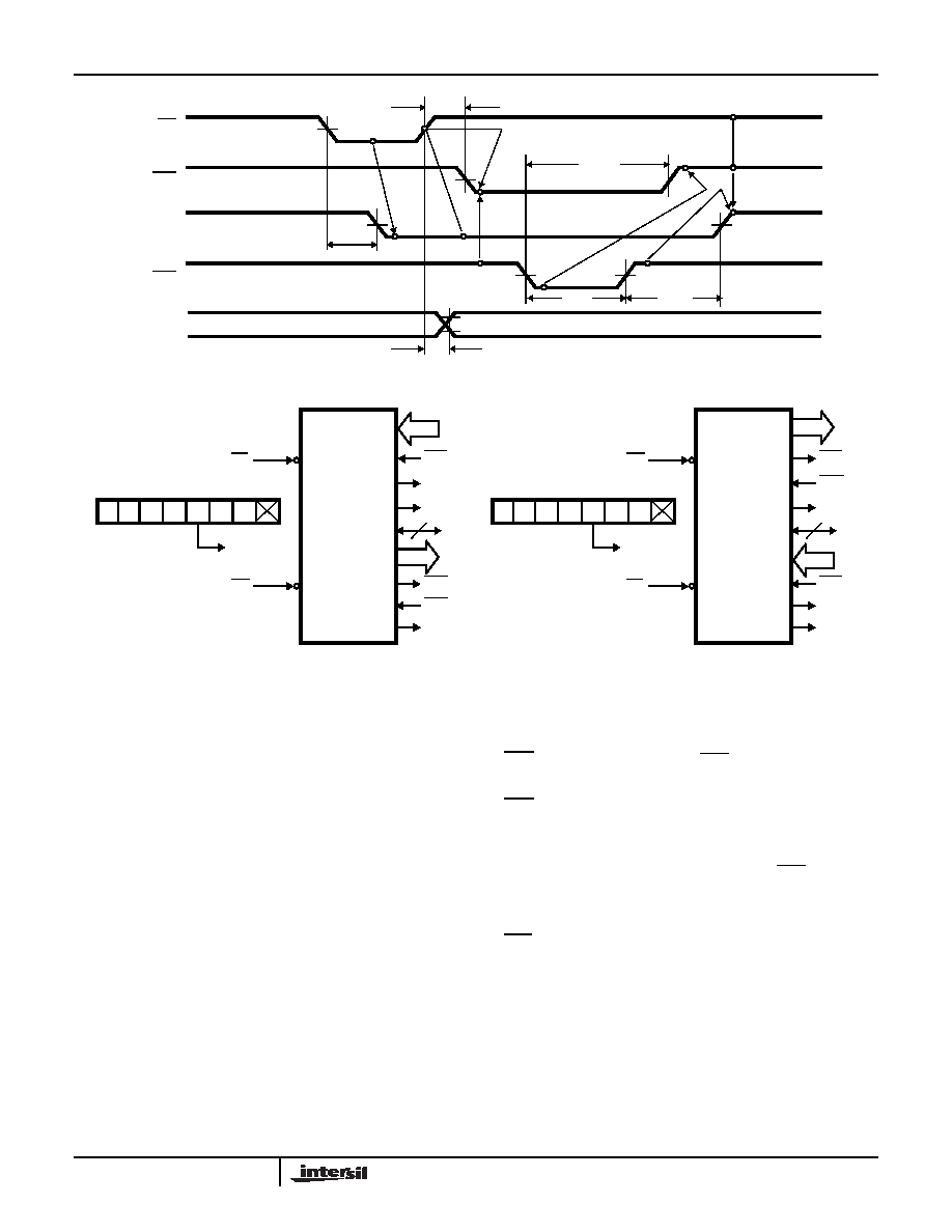
FIGURE 9. MODE 1 (STROBED OUTPUT)
tWOB
tWB
tAK
tAIT
tAOB
tWIT
OBF
WR
INTR
ACK
OUTPUT
Combinations of Mode 1: Port A and Port B can be individually defined as input or output in Mode 1 to support a wide variety of strobed I/O applications.
FIGURE 10. COMBINATIONS OF MODE 1
1
D7
0
D6
1
D5
1
D4
1/0
D3 D2 D1 D0
CONTROL WORD
PORT A - (STROBED INPUT)
PC4
8
OBFB
PA7-PA0
STBA
INTRB
PC0
PC6, PC7
2
WR
PC6, PC7
1 = INPUT
0 = OUTPUT
PORT B - (STROBED OUTPUT)
8
IIBFA
PC5
INTRA
PC3
ACKB
PC2
I/O
PC1
PB7, PB0
RD
10
1
D7
0
D6
1
D5
0
D4
1/0
D3 D2 D1 D0
CONTROL WORD
PORT A - (STROBED OUTPUT)
PC7
8
STBB
PA7-PA0
OBFA
INTRB
PC0
PC4, PC5
2
RD
PC4, PC5
1 = INPUT
0 = OUTPUT
PORT B - (STROBED INPUT)
8
ACKA
PC6
INTRA
PC3
IBFB
PC1
I/O
PC2
PB7, PB0
WR
11
MS82C55A, MQ82C55A, MP82C55A
相关PDF资料 |
PDF描述 |
|---|---|
| PIC18LF2321-I/SP | IC PIC MCU FLASH 4KX16 28DIP |
| DSPIC33FJ12MC201-I/P | IC DSPIC MCU/DSP 12K 20DIP |
| MS27484T22B53P | CONN PLUG 53POS STRAIGHT W/PINS |
| VE-B0V-IX-F2 | CONVERTER MOD DC/DC 5.8V 75W |
| PIC24FJ64GA002-E/SP | IC PIC MCU FLASH 64K 28-SDIP |
相关代理商/技术参数 |
参数描述 |
|---|---|
| CMP93-0-A | 制造商:Thomas & Betts 功能描述:Heat Shrink |
| CMPA0060002F | 功能描述:TRANS RF GAN HEMT MMIC 780019PKG RoHS:是 类别:RF/IF 和 RFID >> RF 放大器 系列:GaN 标准包装:3,000 系列:- 频率:100MHz ~ 6GHz P1dB:9.14dBm(8.2mW) 增益:15.7dB 噪音数据:1.3dB RF 型:CDMA,TDMA,PCS 电源电压:2.7 V ~ 5 V 电流 - 电源:60mA 测试频率:2GHz 封装/外壳:0505(1412 公制) 包装:带卷 (TR) |
| CMPA0060002F-TB | 功能描述:BOARD DEMO AMP CIRC CMPA0060002 RoHS:是 类别:RF/IF 和 RFID >> RF 评估和开发套件,板 系列:GaN 标准包装:1 系列:- 类型:GPS 接收器 频率:1575MHz 适用于相关产品:- 已供物品:模块 其它名称:SER3796 |
| CMPA0060025F | 制造商:Cree 功能描述:IC AMP MMIC HEMT 25W 780019PKG |
| CMPA0060025F-TB | 制造商:Cree 功能描述:BOARD DEMO AMP CKT CMPA0060025F |
发布紧急采购,3分钟左右您将得到回复。