- 您现在的位置:买卖IC网 > PDF目录298954 > COP820C_840C PDF资料下载
参数资料
| 型号: | COP820C_840C |
| 文件页数: | 25/26页 |
| 文件大小: | 352K |
| 代理商: | COP820C_840C |
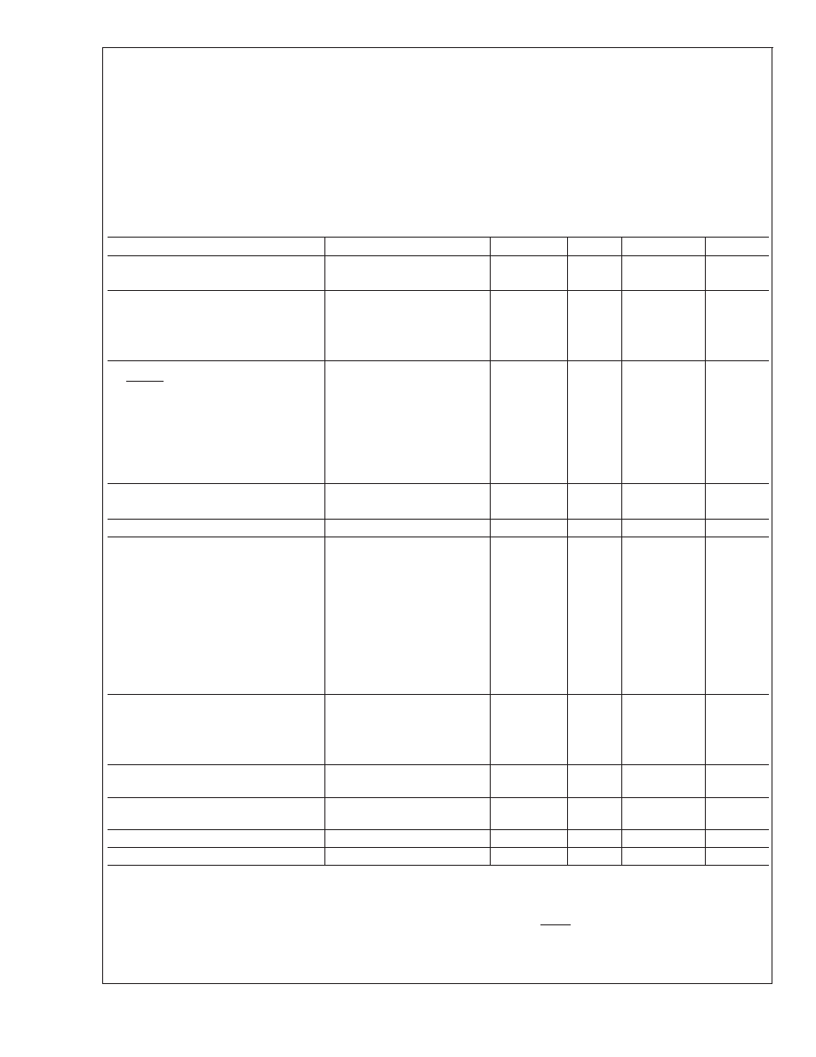
COP620C/COP622C/COP640C/COP642C
Absolute Maximum Ratings (Note 13)
If Military/Aerospace specified devices are required,
please contact the National Semiconductor Sales Office/
Distributors for availability and specifications.
Supply Voltage (V
CC)6V
Voltage at any Pin
0.3V to V
CC + 0.3V
Total Current into V
CC Pin (Source)
40 mA
Total Current out of GND Pin (Sink)
48 mA
Storage Temperature Range
65C to +140C
Note 13:
Absolute maximum ratings indicate limits beyond which damage to
the device may occur. DC and AC electrical specifications are not ensured
when operating the device at absolute maximum ratings.
DC Electrical Characteristics
COP62XC, COP64XC; 55C
≤ T
A ≤ +125C unless otherwise specified
Parameter
Condition
Min
Typ
Max
Units
Operating Voltage
4.5
5.5
V
Power Supply Ripple (Note 14)
Peak to Peak
0.1 V
CC
V
Supply Current (Note 15)
CKI = 10 MHz
V
CC = 5.5V, tc = 1 s
6.0
mA
CKI = 4 MHz
V
CC = 5.5V, tc = 2.5 s
4
mA
HALT Current (Note 16)
V
CC = 5.5V, CKI = 0 MHz
<10
30
A
Input Levels
RESET , CKI
Logic High
0.9 V
CC
V
Logic Low
0.1 V
CC
V
All Other Inputs
Logic High
0.7 V
CC
V
Logic Low
0.2 V
CC
V
Hi-Z Input Leakage
V
CC = 5.5V
5
+5
A
Input Pullup Current
V
CC = 4.5V, VIN = 0V
35
300
A
G Port Input Hysteresis
0.35 V
CC
V
Output Current Levels
D Outputs
Source
V
CC = 4.5V, VOH = 3.8V
0.35
mA
Sink
V
CC = 4.5V, VOL = 1.0V
9
mA
All Others
Source (Weak Pull-Up)
V
CC = 4.5V, VOH = 3.2V
9
120
A
Source (Push-Pull Mode)
V
CC = 4.5V, VOH = 3.8V
0.35
mA
Sink (Push-Pull Mode)
V
CC = 4.5V, VOL = 0.4V
1.4
mA
TRI-STATE Leakage
5.0
+5.0
A
Allowable Sink/Source
Current Per Pin
D Outputs (Sink)
12
mA
All Others
2.5
mA
Maximum Input Current (Room Temp)
Without Latchup (Note 18)
Room Temp
±100
mA
RAM Retention Voltage, Vr
500 ns Rise and Fall Time
(Min)
2.5
V
Input Capacitance
7pF
Load Capacitance on D2
1000
pF
Note 14: Rate of voltage change must be less than 0.5V/ms.
Note 15: Supply current is measured after running 2000 cycles with a square wave CKI input, CKO open, inputs at rails and outputs open.
Note 16: The HALT mode will stop CKI from oscillating in the RC and the Crystal configurations. Test conditions: All inputs tied to VCC, L and G0 — G5 configured
as outputs and set high. The D port set to zero.
Note 17: Except pin G7: +100 mA, 25 mA (COP620C only). Sampled and not 100% tested. Pins G6 and RESET are designed with a high voltage input network
for factory testing. These pins allow input voltages greater than VCC and the pins will have sink current to VCC when biased at voltages greater than VCC (the pins
do not have source current when biased at a voltage below VCC). The effective resistance to VCC is 750 (typical). These two pins will not latch up. The voltage at
the pins must be limited to less than 14V.
COP820C/COP840C
www.national.com
8
相关PDF资料 |
PDF描述 |
|---|---|
| COP820CJMHD-2 | 8-BIT MICROCONTROLLER |
| COP822CJMHD-2 | 8-BIT MICROCONTROLLER |
| COP842CMHD-1 | 8-BIT MICROCONTROLLER |
| COP842CMHD-2 | 8-BIT MICROCONTROLLER |
| COP842CMHD-3 | 8-BIT MICROCONTROLLER |
相关代理商/技术参数 |
参数描述 |
|---|---|
| COP820CJ | 制造商:NSC 制造商全称:National Semiconductor 功能描述:8-Bit Microcontroller with Multi-Input Wake Up and Brown Out Detector |
| COP820CJMHD-2 | 制造商:未知厂家 制造商全称:未知厂家 功能描述:8-Bit Microcontroller |
| COP820CJMHEA-2 | 制造商:未知厂家 制造商全称:未知厂家 功能描述:8-Bit Microcontroller |
| COP820CJ-XXX/M | 制造商:未知厂家 制造商全称:未知厂家 功能描述:8-Bit Microcontroller |
| COP820CJ-XXX/N | 制造商:未知厂家 制造商全称:未知厂家 功能描述:8-Bit Microcontroller |
发布紧急采购,3分钟左右您将得到回复。