- 您现在的位置:买卖IC网 > PDF目录223608 > COP8SGR928V9 (National Semiconductor Corporation) 8-Bit CMOS ROM Based and OTP Microcontrollers with 8k to 32k Memory, Two Comparators and USART PDF资料下载
参数资料
| 型号: | COP8SGR928V9 |
| 厂商: | National Semiconductor Corporation |
| 英文描述: | 8-Bit CMOS ROM Based and OTP Microcontrollers with 8k to 32k Memory, Two Comparators and USART |
| 中文描述: | 8位的CMOS基于ROM和OTP微控制器具有8K到32K的内存,2个比较器和USART |
| 文件页数: | 13/62页 |
| 文件大小: | 913K |
| 代理商: | COP8SGR928V9 |
第1页第2页第3页第4页第5页第6页第7页第8页第9页第10页第11页第12页当前第13页第14页第15页第16页第17页第18页第19页第20页第21页第22页第23页第24页第25页第26页第27页第28页第29页第30页第31页第32页第33页第34页第35页第36页第37页第38页第39页第40页第41页第42页第43页第44页第45页第46页第47页第48页第49页第50页第51页第52页第53页第54页第55页第56页第57页第58页第59页第60页第61页第62页
5.0 Functional Description (Continued)
5.10 OSCILLATOR CIRCUITS
There are four clock oscillator options available: Crystal
Oscillator with or without on-chip bias resistor, R/C Oscillator
with on-chip resistor and capacitor, and External Oscillator.
The oscillator feature is selected by programming the ECON
register, which is summarized in
TABLE 1. Oscillator Option
ECON4
ECON3
Oscillator Option
0
External Oscillator
1
0
Crystal Oscillator without Bias Resistor
0
1
R/C Oscillator
1
Crystal Oscillator with Bias Resistor
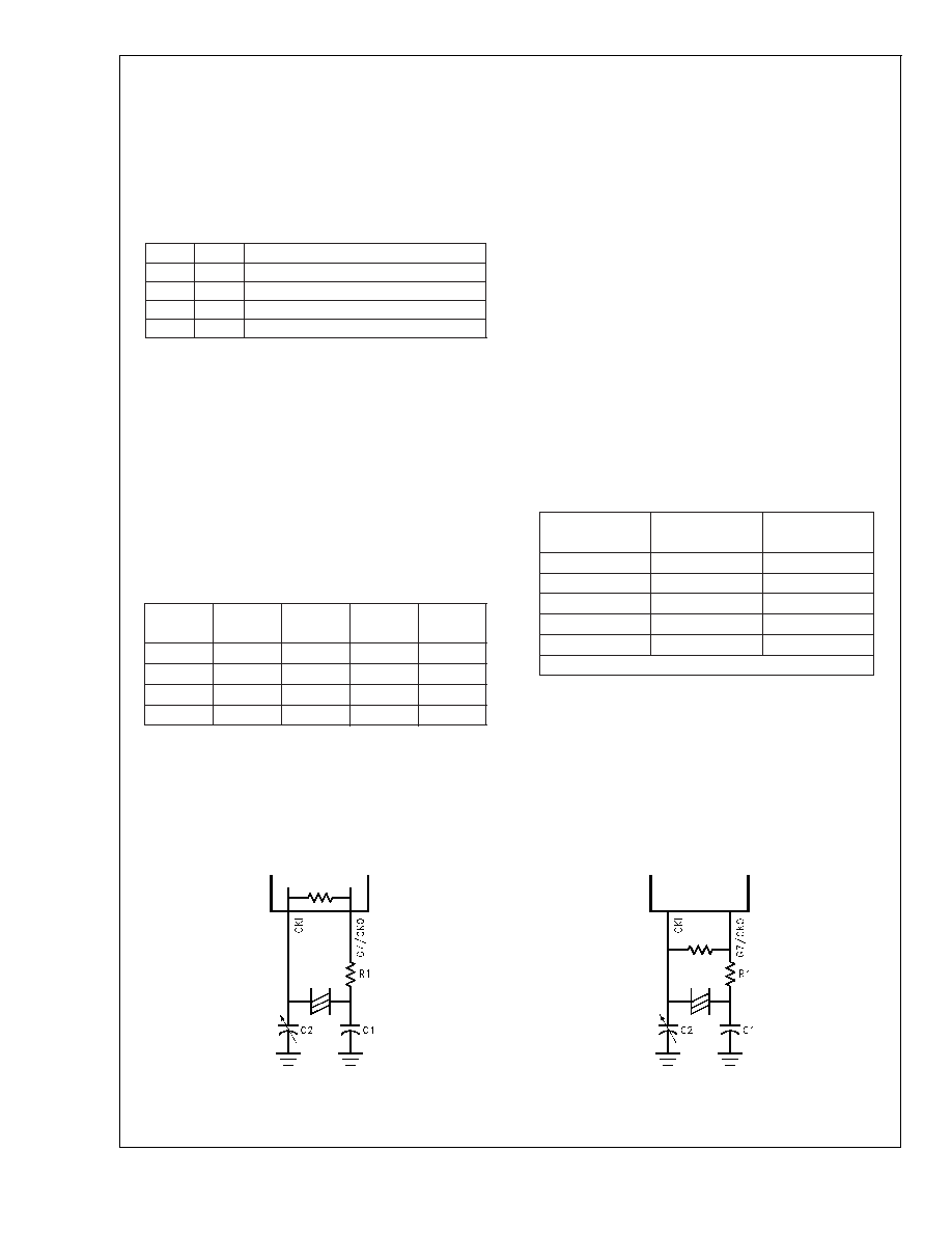
5.10.1 Crystal Oscillator
The crystal Oscillator mode can be selected by programming
ECON Bit 4 to 1. CKI is the clock input while G7/CKO is the
clock generator output to the crystal. An on-chip bias resistor
connected between CKI and CKO can be enabled by pro-
gramming ECON Bit 3 to 1 with the crystal oscillator option
selection. The value of the resistor is in the range of 0.5M to
2M (typically 1.0M).
Table 2 shows the component values
required for various standard crystal values. Resistor R2 is
only used when the on-chip bias resistor is disabled.
12 shows the crystal oscillator connection diagram.
TABLE 2. Crystal Oscillator Configuration,
T
A = 25C, VCC =5V
R1 (k
)R2 (M)
C1 (pF)
C2 (pF)
CKI Freq.
(MHz)
0
1
18
15
0
1
20
10
0
1
25
4
5.6
1
100
100–156
0.455
5.10.2 External Oscillator
The External Oscillator mode can be selected by program-
ming ECON Bit 3 to 0 and ECON Bit 4 to 0. CKI can be
driven by an external clock signal provided it meets the
specified duty cycle, rise and fall times, and input levels.
G7/CKO is available as a general purpose input G7 and/or
Halt control.
Figure 13 shows the external oscillator connec-
tion diagram.
5.10.3 R/C Oscillator
The R/C Oscillator mode can be selected by programming
ECON Bit 3 to 1 and ECON Bit 4 to 0. In R/C oscillation
mode, CKI is left floating, while G7/CKO is available as a
general purpose input G7 and/or HALT control. The R/C
controlled oscillator has on-chip resistor and capacitor for
maximum R/C oscillator frequency operation. The maximum
frequency is 5 MHz ± 35% for V
CC between 4.5V to 5.5V
and temperature range of 40C to +85C. For max fre-
quency operation, the CKI pin should be left floating. For
lower frequencies, an external capacitor should be con-
nected between CKI and either V
CC or GND. Immunity of the
R/C oscillator to external noise can be improved by connect-
ing one half the external capacitance to V
CC and one half to
GND. PC board trace length on the CKI pin should be kept
as short as possible.
Table 3 shows the oscillator frequency
as a function of external capacitance on the CKI pin.
14 shows the R/C oscillator configuration.
TABLE 3. R/C Oscillator Configuration,
40C to +85C, V
CC = 4.5V to 5.5V,
OSC Freq. Variation of ± 35%
External
Capacitor (pF)*
R/C OSC Freq
(MHz)
Instr. Cycle (s)
0
5
2.0
9
4
2.5
52
2
5.0
125
1
10
6100
32 kHz
312.5
* Assumes 3-5 pF board capacitance.
With On-Chip Bias Resistor
Without On-Chip Bias Resistor
10131717
10131718
FIGURE 12. Crystal Oscillator
COP8SG
Family
www.national.com
20
相关PDF资料 |
PDF描述 |
|---|---|
| COPCSH984XXX/WM | 8-BIT, MROM, 10 MHz, MICROCONTROLLER, PDSO28 |
| CP-8-D-2-TS1-TP | INTERCONNECTION DEVICE |
| CP2-SAB1100#NAME | TWO PART BOARD CONNECTOR |
| CP2-SAB1250#NAME | TWO PART BOARD CONNECTOR |
| CP2-SAB950#NAME | TWO PART BOARD CONNECTOR |
相关代理商/技术参数 |
参数描述 |
|---|---|
| COP8-SKFLASH-00 | 功能描述:开发板和工具包 - 其他处理器 DEV STARTER KIT RoHS:否 制造商:Freescale Semiconductor 产品:Development Systems 工具用于评估:P3041 核心:e500mc 接口类型:I2C, SPI, USB 工作电源电压: |
| COP8-SKFLASH-01 | 功能描述:开发板和工具包 - 其他处理器 COP8 5V FLASH STARTER KIT RoHS:否 制造商:Freescale Semiconductor 产品:Development Systems 工具用于评估:P3041 核心:e500mc 接口类型:I2C, SPI, USB 工作电源电压: |
| COP8-SW-COP8C | 制造商:NSC 制造商全称:National Semiconductor 功能描述:8-Bit CMOS Flash Microcontroller with 8k Memory, Dual Op Amps, Virtual EEROM, Temperature Sensor,10-Bit A/D and Brownout Reset |
| COP8-SW-COP8CW | 制造商:NSC 制造商全称:National Semiconductor 功能描述:8-Bit CMOS Flash Microcontroller with 8k Memory, Dual Op Amps, Virtual EEROM, Temperature Sensor,10-Bit A/D and Brownout Reset |
| COP8-SW-EWCOP8 | 制造商:NSC 制造商全称:National Semiconductor 功能描述:8-Bit CMOS Flash Microcontroller with 8k Memory, Dual Op Amps, Virtual EEROM, Temperature Sensor,10-Bit A/D and Brownout Reset |
发布紧急采购,3分钟左右您将得到回复。