- 您现在的位置:买卖IC网 > PDF目录28816 > CPC1590PTR (CLARE INC) PDF资料下载
参数资料
| 型号: | CPC1590PTR |
| 厂商: | CLARE INC |
| 元件分类: | 光电耦合器 |
| 中文描述: | 1 CHANNEL FET OUTPUT OPTOCOUPLER |
| 封装: | ROHS COMPLIANT, FLATPACK-8 |
| 文件页数: | 7/10页 |
| 文件大小: | 372K |
| 代理商: | CPC1590PTR |
CPC1590
6
PRELIMINARY
R00B
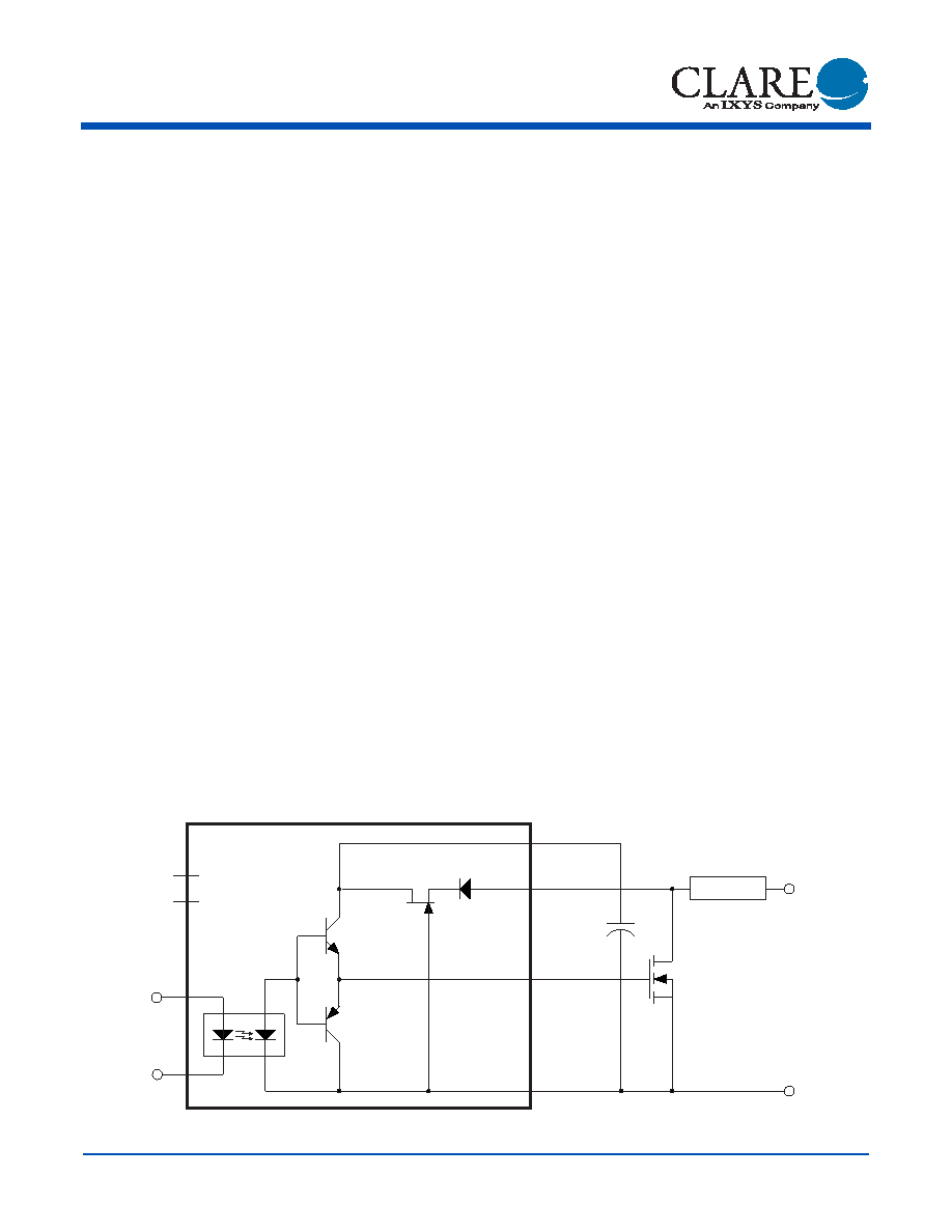
2. Introduction
The CPC1590 is a MOSFET Gate Driver that requires
no external power supply. It can regulate an input
voltage, up to 200V, down to 12.2V for internal use. It
is specifically designed for low-duty-cycle switching
frequencies that drive 4nF of gate capacitance.
3. Functional Description
The CPC1590 is used in conjunction with a single
MOSFET transistor for remote switching of DC loads
(Figure 2), and two MOSFETS and a diode for remote
switching of low-frequency AC loads (Figure 3) where
isolated power is unavailable.
The device uses external components, most notably a
charge storage capacitor, to satisfy design switching
and over-voltage protection requirements. Because of
this design flexibility, the designer may choose a great
number of MOSFETs for use in a wide variety of
applications. The designer simply needs to know the
MOSFET total gate charge (QG), and with this
information a capacitor can be chosen. The
capacitance of the storage capacitor should be greater
than, or equal to, QG/0.5V.
The CPC1590 has two states of operation:
(1) sufficient input control current is flowing, the LED is
turned on, and the gate current is being applied. The
light from the LED is being reflected onto the
photovoltaic, which then produces a photocurrent that
turns on the NPN bipolar transistor and provides the
charge (I x t = Q), or the gate current that is being
applied to turn on the MOSFET. (2) Sufficient input
control current is not flowing, the LED is turned off,
and gate current is not flowing. The LED is off
because VF << the minimum forward voltage required,
and not enough current is being applied. This turns on
the PNP bipolar transistor, providing a path for gate
current to discharge to VL2.
When VLOAD is first applied, the external storage
capacitor begins to charge. The charge is sent through
a bootstrap diode to prevent the charge from escaping
and discharging through a turned-on MOSFET. The
J-FET then regulates the voltage between 10V and
16V. The input control current is applied, then the
charge is transferred from the storage capacitor
through the NPN bipolar transistor, along with the
charge from the photovoltaic, to the MOSFET gate to
accomplish a rapid turn-on. After the capacitor has
discharged and the MOSFET has turned on, the
photocurrent from the input optocoupler continues to
flow into the gate to keep the MOSFET turned on.
When the input control current is removed, the gate
current stops flowing and the PNP bipolar transistor is
on and is discharging the MOSFET gate. The
MOSFET is now off. At this point the capacitor begins
to recharge for the next turn on cycle.
The circuit below does not include over-voltage
protection.
Figure 2. CPC1590 DC Application Circuit
2
3
1
4
NC
8
5
6
7
CPC1590
LED +
LED -
V
CAP
+V
LOAD
V
G
-V
LOAD
C
ST
LOAD
V
L1
V
L2
相关PDF资料 |
PDF描述 |
|---|---|
| CPC1726Y | |
| CPC1788J | |
| CPC1961GSTR | |
| CPC1961GS | |
| CPC1963GSTR | |
相关代理商/技术参数 |
参数描述 |
|---|---|
| CPC1593 | 制造商:IXYS 制造商全称:IXYS Corporation 功能描述:Single-Pole, Normally Open OptoMOS?? Relay Integrated Current Limit with Voltage and Thermal Protection |
| CPC1593G | 功能描述:固态继电器-PCB安装 1-Form-A 600V 6-Pin DIP RoHS:否 制造商:Omron Electronics 控制电压范围: 负载电压额定值:40 V 负载电流额定值:120 mA 触点形式:1 Form A (SPST-NO) 输出设备:MOSFET 封装 / 箱体:USOP-4 安装风格:SMD/SMT |
| CPC1593GS | 功能描述:固态继电器-PCB安装 1-Form-A 600V 6-Pin SM RoHS:否 制造商:Omron Electronics 控制电压范围: 负载电压额定值:40 V 负载电流额定值:120 mA 触点形式:1 Form A (SPST-NO) 输出设备:MOSFET 封装 / 箱体:USOP-4 安装风格:SMD/SMT |
| CPC1593GSTR | 功能描述:固态继电器-PCB安装 1-Form-A 600V 6-Pin SM T/R RoHS:否 制造商:Omron Electronics 控制电压范围: 负载电压额定值:40 V 负载电流额定值:120 mA 触点形式:1 Form A (SPST-NO) 输出设备:MOSFET 封装 / 箱体:USOP-4 安装风格:SMD/SMT |
| CPC15AC | 功能描述:板上安装压力/力传感器 ASG/SENSYM 130 - CPC,CPCL RoHS:否 制造商:Honeywell 工作压力:0 bar to 4 bar 压力类型:Gage 准确性:+ / - 0.25 % 输出类型:Digital 安装风格:Through Hole 工作电源电压:5 V 封装 / 箱体:SIP 端口类型:Dual Radial Barbed, Same sides |
发布紧急采购,3分钟左右您将得到回复。