- 您现在的位置:买卖IC网 > PDF目录28817 > CS1500-FSZ (CIRRUS LOGIC INC) PDF资料下载
参数资料
| 型号: | CS1500-FSZ |
| 厂商: | CIRRUS LOGIC INC |
| 元件分类: | 稳压器 |
| 中文描述: | 0.5 A POWER FACTOR CONTROLLER, 70 kHz SWITCHING FREQ-MAX, PDSO8 |
| 封装: | 0.150 INCH, LEAD FREE, MS-012, SOIC-8 |
| 文件页数: | 14/14页 |
| 文件大小: | 201K |
| 代理商: | CS1500-FSZ |
CS1500
DS849F1
9
Nov ?$shortyear>
CONFIDENTIAL
5.4 Output Power and PFC Boost Inductor
In normal operating mode, the nominal output power is
estimated by the following equation.
where:
Po
rated output power of the system
η
efficiency of the boost converter (estimated as 100%
by the PFC algorithm)
Vin(min) minimum RMS line voltage is 90V, measured after
the rectifier and EMI filter
Vlink
nominal PFC output voltage must be 400 V
fmax
maximum switching frequency is 70 kHz
LB
boost inductor specified by rated power requirement
α
margin factor to guarantee rated output power (Po)
against boost inductor tolerances.
Equation 1 is provided for explanation purposes only. Using
substituted required design values for Vlink and fmax gives the
following equation.
Changing values for application-specific devices such as the
boost inductor or Vlink voltage is not recommended and
requires changing internal register values.
Solving Equation 2 for the PFC boost inductor LB gives the
following equation.:
If a value of the boost inductor other than that obtained from
Equation 3 above is used, the total output power capability as
well as the minimum input voltage threshold will differ
according to Equation 2.
Figure 15. Relative Effects of Varying Boost Inductance
5.5 PFC Output Capacitor
The value of the PFC output capacitor should be chosen
based upon voltage ripple and hold-up requirements. To
ensure system stability with the digital controller, the
recommended value of the capacitor is within the range of
0.5
μF / watt to 2.0 μF/watt.
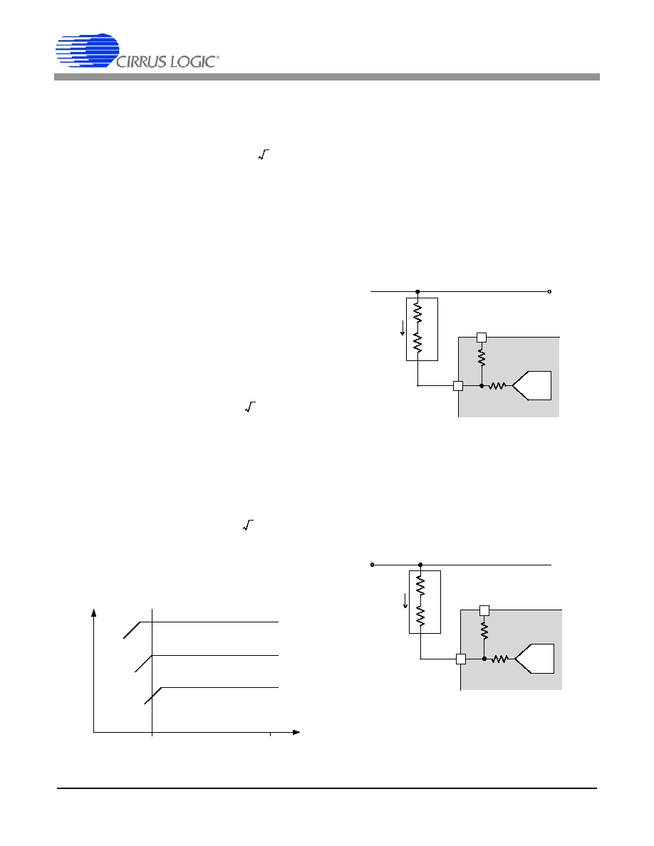
5.6 Output IFB Sense & Input IAC Sense
A current proportional to the PFC output voltage, Vlink, is
supplied to the IC on pin IFB and is used as a feedback control
signal. This current is compared against an internal fixed-
value current.
The ADC is used to measure the magnitude of the IFB current
through resistor RIFB. The magnitude of the IFB current is then
compared to an internal fixed-value current.
Figure 16. Feedback Input Pin Model
Resistor RIFB sets the feedback current and is calculated as
follows:
By using digital loop compensation, the voltage feedback
signal does not require an external compensation network.
A current proportional to the AC input voltage is supplied to the
IC on pin IAC and is used by the PFC control algorithm.
Figure 17. IAC Input Pin Model
Resistor RIAC sets the IAC current and is derived as follows:
For optimal performance, resistors RIAC & RIFB should use 1%
tolerance or better resistors.
Po
αη
V
in min
()
×
2
×
V
link
V
in min
()
2
×
()
–
2f
max
L
B
V
link
×
---------------------------------------------------------
×
=
[Eq.1]
Po
αη
90V
()
×
2
×
400V
90V
2
×
()
–
270kHz
L
B
400V
×
-------------------------------------------------------------
×
=
[Eq.2]
L
B
αη
90V
()
×
2
×
400V
90V
2
×
()
–
270kHz
Po
400V
×
-------------------------------------------------------------
×
=
[Eq.3]
VAC(rms)
90
265
P
o(
m
a
x
)
L > LB
/α
L = LB
L < LB
/α
IFB
VDD
15k
7
Vlink
CS1500
24k
ADC
R3
RIFB
IFB
R4
4
R
IFB
V
link
V
dd
–
I
fixed
----------------------------
400V
V
dd
–
129
μA
------------------------------
==
[Eq.4]
R1
RIAC
IAC
IA C
VDD
15k
7
Vrect
CS1500
24k
ADC
R2
3
R
IAC
R
IFB
=
[Eq.5]
相关PDF资料 |
PDF描述 |
|---|---|
| CS1600-FSZ | |
| CS2000P-DZZR | |
| CS2100CP-DZZR | |
| CS2200CP-DZZR | |
| CS2300CP-DZZR | |
相关代理商/技术参数 |
参数描述 |
|---|---|
| CS1501 | 制造商:CIRRUS 制造商全称:Cirrus Logic 功能描述:Digital Power Factor Correction Control IC |
| CS1501-7R | 功能描述:EURO-CASSETTE 100W 15V RoHS:否 类别:电源 - 外部/内部(非板载) >> DC DC Converters 系列:* 标准包装:1 系列:Quint 类型:隔离 输入电压:24V 输出:24V 输出数:1 输出 - 1 @ 电流(最大):24 VDC @ 50A 输出 - 2 @ 电流(最大):- 输出 - 3 @ 电流(最大):- 输出 - 4 @ 电流(最大):- 功率(瓦特):1200W 安装类型:底座安装 工作温度:0°C ~ 40°C 效率:- 封装/外壳:模块 尺寸/尺寸:4.33" L x 9.09" W x 6.14" H(110mm x 231mm x 156mm) 包装:散装 电源(瓦特)- 最大:1200W 批准:- 其它名称:277-69722866365-NDQUINT-BAT/24DC/12AH |
| CS1501-9ER | 制造商:Power-One 功能描述:DCDC - Bulk |
| CS1501-FSZ | 功能描述:功率因数校正 IC DIGITAL PFC CONT. IC FOR SMPS RoHS:否 制造商:Fairchild Semiconductor 开关频率:300 KHz 最大功率耗散: 最大工作温度:+ 125 C 安装风格:SMD/SMT 封装 / 箱体:SOIC-8 封装:Reel |
| CS1501-FSZR | 制造商:Cirrus Logic 功能描述:IC PFC CONTROLLER DCM OCP - Tape and Reel 制造商:Cirrus Logic 功能描述:IC PFC CTRLR DCM OCP 8SOIC 制造商:Cirrus Logic 功能描述:PFC Controller |
发布紧急采购,3分钟左右您将得到回复。