- 您现在的位置:买卖IC网 > PDF目录380066 > CS4124 (ON SEMICONDUCTOR) High Side PWM FET Controller(高端PWM FET控制器) PDF资料下载
参数资料
| 型号: | CS4124 |
| 厂商: | ON SEMICONDUCTOR |
| 英文描述: | High Side PWM FET Controller(高端PWM FET控制器) |
| 中文描述: | 高侧FET的控制器的PWM(脉宽调制高端场效应管控制器) |
| 文件页数: | 7/12页 |
| 文件大小: | 86K |
| 代理商: | CS4124 |
CS4124
http://onsemi.com
7
APPLICATIONS INFORMATION
THEORY OF OPERATION
Oscillator
The IC sets up a constant frequency triangle wave at the
C
OSC
lead whose frequency is related to the external
components R
OSC
and C
OSC
, by the following equation:
Frequency
0.83
ROSC
COSC
The peak and valley of the triangle wave are proportional
to V
CC
by the following:
VVALLEY
0.1
VCC
VPEAK
0.7
VCC
This is required to make the voltage compensation
function properly. In order to keep the frequency of the
oscillator constant the current that charges C
OSC
must also
vary with supply. R
OSC
sets up the current which charges
C
OSC
. The voltage across R
OSC
is 50% of V
CC
and
therefore:
IROSC
0.5
VCC
ROSC
I
ROSC
is multiplied by (2) internally and transferred to the
C
OSC
lead. Therefore:
ICOSC
VCC
ROSC
The period of the oscillator is:
T
2COSC
VPEAK
VVALLEY
ICOSC
The R
OSC
and C
OSC
components can be varied to create
frequencies over the range of 15 Hz to 25 kHz. With the
suggested values of 93.1 k
and 470 pF for R
OSC
and C
OSC
,
the nominal frequency will be approximately 20 kHz.
I
ROSC
, at V
CC
= 14 V, will be 66.7
μ
A. I
ROSC
should not
change over a more than 2:1 ratio and therefore C
OSC
should
be changed to adjust the oscillator frequency.
Voltage Duty Cycle Conversion
The IC translates an input voltage at the CTL lead into a
duty cycle at the OUTPUT lead. The transfer function
incorporates ON Semiconductor’s patented Voltage
Compensation method to keep the average voltage and
current across the load constant regardless of fluctuations in
the supply voltage. The duty cycle is varied based upon the
input voltage and supply voltage by the following equation:
Duty Cycle
100%
2.8
VCTL
VCC
An internal DC voltage equal to:
VDC
(1.683
VCTL)
VVALLEY
is compared to the oscillator voltage to produce the
compensated duty cycle. The transfer is set up so that when
V
CC
= 14 V the duty cycle will equal V
CTL
divided by V
REG
.
For example at V
CC
= 14 V, V
REG
= 5.0 V and V
CTL
= 2.5 V,
the duty cycle would be 50% at the output. This would place
a 7.0 V average voltage across the load. If V
CC
then drops
to 10 V, the IC would change the duty cycle to 70% and
hence keep the average load voltage at 7.0 V.
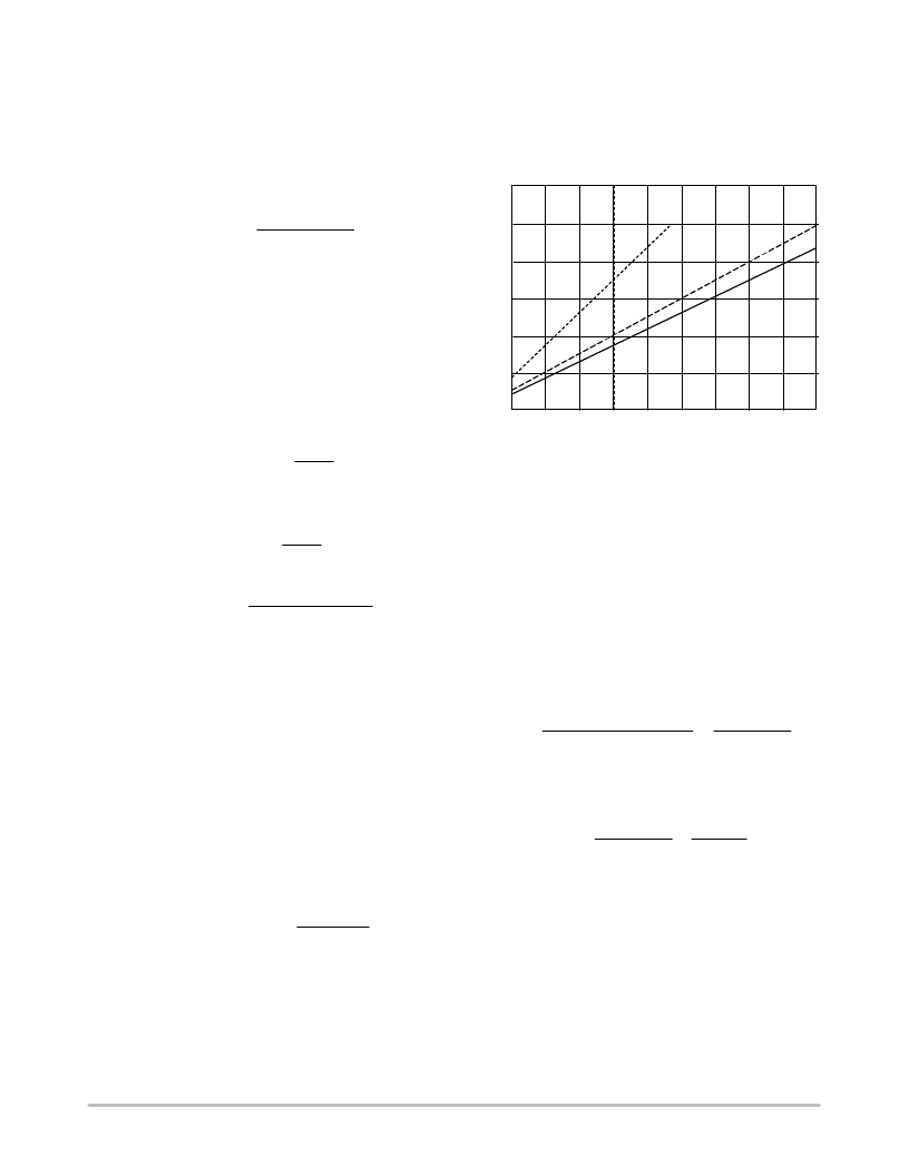
10
20
30
40
50
60
70
80
90
CTL Voltage (% of V
REG
)
Figure 7. Voltage Compensation
100
0
20
40
60
80
100
120
D
V
CC
= 8.0 V
V
CC
= 14 V
V
CC
= 16 V
5.0 V Linear Regulator
There is a 5.0 V, 5.0 mA linear regulator available at the
V
REG
lead for external use. This voltage acts as a reference
for many internal and external functions. It has a drop out of
approximately 1.5 V at room temperature.
Current Sense and Timer
The IC differentially monitors the load current on a cycle
by cycle basis at the I
SENSE+
and I
SENSE–
leads. The
differential voltage across these two leads is amplified
internally and compared to the voltage at the I
ADJ
lead. The
gain, A
V
is set internally and externally by the following
equation:
VI(ADJ)
ISENSE
ISENSE
AV
37000
1000
RCS
The current limit (I
LIM
) is set by the external current sense
resistor (R
SENSE
) placed across the I
SENSE+
and I
SENSE–
terminals and the voltage at the I
ADJ
lead.
ILIM
1000
RCS
37000
VI(ADJ)
RSENSE
The R
CS
resistors and C
CS
components form a differential
low pass filter which filters out high frequency noise
generated by the switching of the external MOSFET and the
associated lead noise. R
CS
also forms an error term in the
gain of the I
LIM
equation because the I
SENSE+
and I
SENSE–
leads are low impedance inputs thereby creating a good
current sensing amplifier. Both leads source 50
μ
A while the
chip is in run mode. I
ADJ
should be biased between 1.0 V and
4.0 V. When the current through the external MOSFET
exceeds I
LIM
, an internal latch is set and the output pulls the
gate of the MOSFET low for the remainder of the oscillator
cycle (fault mode). At the start of the next cycle, the latch is
相关PDF资料 |
PDF描述 |
|---|---|
| CS4161 | 85 mA Dual H-Bridge Stepper Motor Driver(85mA双H-桥步进电机驱动器) |
| CS4192XDWF16G | Single Air−Core Gauge Driver |
| CS4192XDWFR16G | Single Air−Core Gauge Driver |
| CS4192 | Single Air-Core Gauge Driver |
| CS4192XDWF16 | Single Air-Core Gauge Driver |
相关代理商/技术参数 |
参数描述 |
|---|---|
| CS4124/D | 制造商:未知厂家 制造商全称:未知厂家 功能描述:High Side PWM FET Controller |
| CS-4124N16 | 制造商:未知厂家 制造商全称:未知厂家 功能描述:DC Motor Controller/Driver |
| CS4124YN16 | 功能描述:IC REG CTRLR BST PWM 16-DIP RoHS:否 类别:集成电路 (IC) >> PMIC - 稳压器 - DC DC 切换控制器 系列:- 标准包装:4,000 系列:- PWM 型:电压模式 输出数:1 频率 - 最大:1.5MHz 占空比:66.7% 电源电压:4.75 V ~ 5.25 V 降压:是 升压:无 回扫:无 反相:无 倍增器:无 除法器:无 Cuk:无 隔离:无 工作温度:-40°C ~ 85°C 封装/外壳:40-VFQFN 裸露焊盘 包装:带卷 (TR) |
| CS-4-12XA | 制造商:Nidec Copal 功能描述:SWIT ROTARY SP SLOT J-HOOK 0.1A 16VAC 16VDC 0.5W - Bulk |
| CS-4-12XB | 制造商:Nidec Copal 功能描述:SWIT ROTARY SP SCRWDRVR GW 0.1A 16VAC 16VDC 0.5W - Bulk 制造商:Nidec Copal 功能描述:Switches, rotary, surface mount, |
发布紧急采购,3分钟左右您将得到回复。