- 您现在的位置:买卖IC网 > PDF目录380066 > CS4216 (Cirrus Logic, Inc.) 16-Bit Stereo Audio Codec PDF资料下载
参数资料
| 型号: | CS4216 |
| 厂商: | Cirrus Logic, Inc. |
| 元件分类: | Codec |
| 英文描述: | 16-Bit Stereo Audio Codec |
| 中文描述: | 16位立体声音频编解码器 |
| 文件页数: | 13/58页 |
| 文件大小: | 799K |
| 代理商: | CS4216 |
第1页第2页第3页第4页第5页第6页第7页第8页第9页第10页第11页第12页当前第13页第14页第15页第16页第17页第18页第19页第20页第21页第22页第23页第24页第25页第26页第27页第28页第29页第30页第31页第32页第33页第34页第35页第36页第37页第38页第39页第40页第41页第42页第43页第44页第45页第46页第47页第48页第49页第50页第51页第52页第53页第54页第55页第56页第57页第58页
Sub-frame Bits 17 to 24
17
18
19
20
21
0
22
ADV
23
LCL
24
RCL
RESERVED
ADV
ADC Valid data bit.
0- Invalid ADC data
1- Valid ADC data
Indicates ADC has completed initialization
after power-up, low power mode,
or mute.
LCL
Left ADC clipping indicator
0- Normal
1- Clipping
Right ADC clipping indicator
0- Normal
1- Clipping
RESERVED bits can be 0 or 1
RCL
Sub-frame Bits 25 to 32
25
ER3
26
ER2
27
ER1
28
ER0
29
Ver3
30
Ver2
31
Ver1
32
Ver0
ER3-ER0 Error Word
0000 - Normal – No errors.
0001 - Input Sub-frame Bit 21 is set.
Control data will not be loaded
0010 - Sync Pulse is incorrect.
Causes the analog output to mute.
0011 - SCLK is outside the allowable
range. Analog output mutes.
CS4216 Version Number
0000 = "A" (see Appendix A)
0001 = "B", "C", . . . (This data sheet)
Ver3-Ver0
Sub-frame Bits 33 to 48
Right ADC Audio Data, MSB first, 2’s comple-
ment coded.
Sub-frame Bits 1 to 16
Left ADC Audio Data, MSB first, 2’s comple-
ment coded.
OUTPUT DATA BIT DEFINITIONS
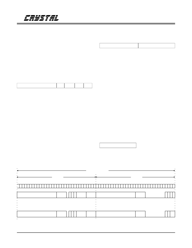
6
ADC - Left Word
3
0 3
0
0
A
ADC - Right Word
Sub-frame
Word B
Word A
ADC - Left Word
3
0 3
0
0
SM1 and SM2
SM3
ADC - Right Word
D
D
X X
M
M
L
L
A
L
R
Error
Error
Version
Version
M
M
L
L
0 0 0 1 0 0 0 0
0 0 0 1 0 0 0 0
D
D
D
D
0
1
1
2
2
2
2
2
3
2
2
3
5
4
5
5
5
6
6
5
L
R
. X X X
X X X X
X X X X
X X X X
Figure 6. Serial Data Output Format - SM1, SM2, and SM3.
Sub-frame Bits 49 to 60
These bits are reserved, and can be 0 or 1.
Sub-frame Bits 61 to 64
61
DI1
62
DI2
63
DI3
64
DI4
DI1-DI4
These bits follow the state of the Digital
Input pins. In SM3 DI3 and DI4 are used
and unavailable. In SM4 DI2, DI3, & DI4
are not available as input bits.
CS4216
DS83F2
13
相关PDF资料 |
PDF描述 |
|---|---|
| CS4216-KL | IC EEPROM SRL 256-8BIT 8DIP |
| CS4216-KQ | 16-Bit Stereo Audio Codec |
| CS4218-KL | 16-Bit Stereo Audio Codec |
| CS4218-KQ | 16-Bit Stereo Audio Codec |
| CS4218 | 16-Bit Stereo Audio Codec |
相关代理商/技术参数 |
参数描述 |
|---|---|
| CS4216-KL | 制造商:Rochester Electronics LLC 功能描述:- Bulk |
| CS4216-KQ | 制造商:CIRRUS 制造商全称:Cirrus Logic 功能描述:16-Bit Stereo Audio Codec |
| CS4217-KL | 制造商:CRYSTAL 功能描述: |
| CS4218 | 制造商:CIRRUS 制造商全称:Cirrus Logic 功能描述:16-Bit Stereo Audio Codec |
| CS4218-KL | 制造商:CIRRUS 制造商全称:Cirrus Logic 功能描述:16-Bit Stereo Audio Codec |
发布紧急采购,3分钟左右您将得到回复。