- 您现在的位置:买卖IC网 > PDF目录10940 > CS42L55-CNZR (Cirrus Logic Inc)IC CODEC STER H-HDPN AMP 36-QFN PDF资料下载
参数资料
| 型号: | CS42L55-CNZR |
| 厂商: | Cirrus Logic Inc |
| 文件页数: | 25/68页 |
| 文件大小: | 0K |
| 描述: | IC CODEC STER H-HDPN AMP 36-QFN |
| 标准包装: | 6,000 |
| 类型: | 立体声音频 |
| 数据接口: | 串行 |
| 分辨率(位): | 24 b |
| ADC / DAC 数量: | 1 / 1 |
| 三角积分调变: | 是 |
| 动态范围,标准 ADC / DAC (db): | 95 / 99 |
| 电压 - 电源,模拟: | 1.65 V ~ 2.71 V |
| 电压 - 电源,数字: | 1.65 V ~ 2.71 V |
| 工作温度: | -40°C ~ 85°C |
| 安装类型: | 表面贴装 |
| 封装/外壳: | 36-QFN |
| 供应商设备封装: | 36-QFN-EP(5x5) |
| 包装: | 带卷 (TR) |
| 配用: | 598-1506-ND - BOARD EVAL FOR CS42L55 CODEC |
第1页第2页第3页第4页第5页第6页第7页第8页第9页第10页第11页第12页第13页第14页第15页第16页第17页第18页第19页第20页第21页第22页第23页第24页当前第25页第26页第27页第28页第29页第30页第31页第32页第33页第34页第35页第36页第37页第38页第39页第40页第41页第42页第43页第44页第45页第46页第47页第48页第49页第50页第51页第52页第53页第54页第55页第56页第57页第58页第59页第60页第61页第62页第63页第64页第65页第66页第67页第68页
October 2004
31
M9999-101204
MIC3000
Micrel
Serial Port Operation
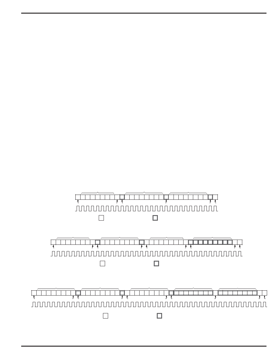
The MIC3000 uses standard Write_Byte, Read_Byte, and
Read_Word operations for communication with its host. It
also supports Page_Write and Sequential_Read transac-
tions. The Write_Byte operation involves sending the device’s
slave address (with the R/W bit low to signal a write opera-
tion), followed by the address of the register to be operated
upon and the data byte. The Read_Byte operation is a
composite write and read operation: the host first sends the
device’s slave address followed by the register address, as in
a write operation. A new start bit must then be sent to the
MIC3000, followed by a repeat of the slave address with the
R/W bit (LSB) set to the high (read) state. The data to be read
from the part may then be clocked out. A Read_Word is
similar, but two successive data bytes are clocked out rather
than one. These protocols are shown in Figure 21 to 24.
The MIC3000 will respond to up to four sequential slave
addresses depending upon whether it is in OEM or User
mode. A match between one of the MIC3000’s addresses
and the address specified in the serial bit stream must be
made to initiate communication. The MIC3000 responds to
slave addresses A0h and A2h in User Mode; it also responds
to A4h and A6h in OEM Mode (assuming I2CADR = Axh).
Page Writes
To increase the speed of multi-byte writes, the MIC3000
allows up to four consecutive bytes (one page) to be written
before the internal write cycle begins. The entire non-volatile
memory array is organized into four-byte pages. Each page
begins on a register address boundary where the last two bits
of the address are 00b. Thus the page is composed of any four
consecutive bytes having the addresses xxxxxx00b,
xxxxxx01b, xxxxxx10b, and xxxxxx11b.
The page write sequence begins just like a Write_Byte
operation with the host sending the slave address, R/W bit
low, register address, etc. After the first byte is sent the host
should receive an acknowledge. Up to three more bytes can
be sent in sequence. The MIC3000 will acknowledge each
one and increment its internal address register in anticipation
of the next byte. After the last byte is sent, the host issues a
STOP. The MIC3000’s internal write process then begins. If
more than four bytes are sent, the MIC3000’s internal ad-
dress counter wraps around to the beginning of the four-byte
page.
To accelerate calibration and testing, NVRAM write cycles
can be disabled completely by setting the WRINH bit in
OEMCAL0. Writes to registers that do not have NVRAM
backup will not incur write-cycle delays when writes are
inhibited. Write operations on registers that exist only in
NVRAM will still incur write cycle delays.
S 1010
000
0 AXXXXXXXXA
D4
D5
D6
D3 D2 D1 D0
D7
/A P
MIC3000 Slave Address
DATA
CLK
Register Address
Data Byte to MIC3000
START
STOP
R/W = WRITE
ACKNOWLEDGE
NOT ACKNOWLEDGE
Master to slave transfer,
i.e., DATA driven by master.
Slave to master transfer,
i.e., DATA driven by slave.
Figure 21. Write Byte Protocol
S 1010000
X X A0
0 A 0
0 XXXXXXAS 1
1
00
X
XXXX
A X
/A P
MIC3000 Slave Address
DATA
CLK
Register Address
MIC3000 Slave Address
Data Read From MIC3000
START
STOP
R/W = WRITE
R/W = READ
ACKNOWLEDGE
NOT ACKNOWLEDGE
Master to slave transfer,
i.e., DATA driven by master.
Slave to master transfer,
i.e., DATA driven by slave.
Figure 22. Read Byte Protocol
S 1010
000
0 A 000000 X X A
MIC3000 Slave Address
DATA
CLK
Register Address
START
R/W = WRITE
ACKNOWLEDGE
S 1010
000
1A
A
D3
D4
D5
D2 D1 D0
D7
D6
D7
/A P
D6 D5 D4 D3 D2 D1 D0
MIC3000 Slave Address
High-Order Byte
from MIC3000
Low-Order Byte
from MIC3000
START
STOP
R/W = READ
ACKNOWLEDGE
NOT ACKNOWLEDGE
Master-to-slave tranfer,
i.e., DATA driven by master.
Slave-to-master transfer,
i.e.,DATA driven by slave.
Figure 23. Read_Word Protocol
相关PDF资料 |
PDF描述 |
|---|---|
| DSP56F807VF80 | IC DSP 80MHZ 60K FLASH 160-BGA |
| VI-B20-IW-B1 | CONVERTER MOD DC/DC 5V 100W |
| MC9328MXLCVM15 | IC MCU I.MXL 150MHZ 256-MAPBGA |
| VI-2NX-CU-S | CONVERTER MOD DC/DC 5.2V 200W |
| CS42L51-CNZR | IC CODEC LOW-V 24BIT 32-QFP |
相关代理商/技术参数 |
参数描述 |
|---|---|
| CS42L55-DNZ | 功能描述:接口—CODEC Portble Stereo CODEC Class H HP Amp RoHS:否 制造商:Texas Instruments 类型: 分辨率: 转换速率:48 kSPs 接口类型:I2C ADC 数量:2 DAC 数量:4 工作电源电压:1.8 V, 2.1 V, 2.3 V to 5.5 V 最大工作温度:+ 85 C 安装风格:SMD/SMT 封装 / 箱体:DSBGA-81 封装:Reel |
| CS42L55DNZR | 制造商:Cirrus Logic 功能描述:PORTABLE STEREO CODEC AND UNIQUE CLASS H HP AMP AUTO GRADE & - Tape and Reel |
| CS42L55-DNZR | 功能描述:接口—CODEC Portable Ster CODEC w/Class H HP Amp RoHS:否 制造商:Texas Instruments 类型: 分辨率: 转换速率:48 kSPs 接口类型:I2C ADC 数量:2 DAC 数量:4 工作电源电压:1.8 V, 2.1 V, 2.3 V to 5.5 V 最大工作温度:+ 85 C 安装风格:SMD/SMT 封装 / 箱体:DSBGA-81 封装:Reel |
| CS42L56-CNZ | 功能描述:接口—CODEC IC 24Bit UltraLowPwr Ster Codec w/clH HP RoHS:否 制造商:Texas Instruments 类型: 分辨率: 转换速率:48 kSPs 接口类型:I2C ADC 数量:2 DAC 数量:4 工作电源电压:1.8 V, 2.1 V, 2.3 V to 5.5 V 最大工作温度:+ 85 C 安装风格:SMD/SMT 封装 / 箱体:DSBGA-81 封装:Reel |
| CS42L56-CNZR | 功能描述:接口—CODEC IC 24Bit UltraLowPwr Ster CD w/clH HP RoHS:否 制造商:Texas Instruments 类型: 分辨率: 转换速率:48 kSPs 接口类型:I2C ADC 数量:2 DAC 数量:4 工作电源电压:1.8 V, 2.1 V, 2.3 V to 5.5 V 最大工作温度:+ 85 C 安装风格:SMD/SMT 封装 / 箱体:DSBGA-81 封装:Reel |
发布紧急采购,3分钟左右您将得到回复。