- 您现在的位置:买卖IC网 > PDF目录223611 > CS5101EN14 1.5 A SWITCHING CONTROLLER, PDIP14 PDF资料下载
参数资料
| 型号: | CS5101EN14 |
| 元件分类: | 稳压器 |
| 英文描述: | 1.5 A SWITCHING CONTROLLER, PDIP14 |
| 封装: | PLASTIC, DIP-14 |
| 文件页数: | 5/7页 |
| 文件大小: | 155K |
| 代理商: | CS5101EN14 |
5
CS5101
Circuit Description: continued
The CS5101 is designed to regulate voltages in multiple
output power supplies. Functionally, it is similar to a
magnetic amplifier, operating as a switch with a delayed
turn-on. It can be used with both single ended and dual
ended topologies.
The VFB voltage is monitored by the error amplifier EA. It
is compared to an internal reference voltage and the
amplified differential signal is fed through an inverting
amplifier into the buffer, BUF. The buffered signal is com-
pared at the PWM comparator with the ramp voltage
generated by capacitor CR. When the ramp voltage VR,
exceeds the control voltage VC, the output of the PWM
comparator goes high, latching its state through the
LATCH, the output stage transistor Q1 turns on, and the
external power switch, usually an N-FET, turns on.
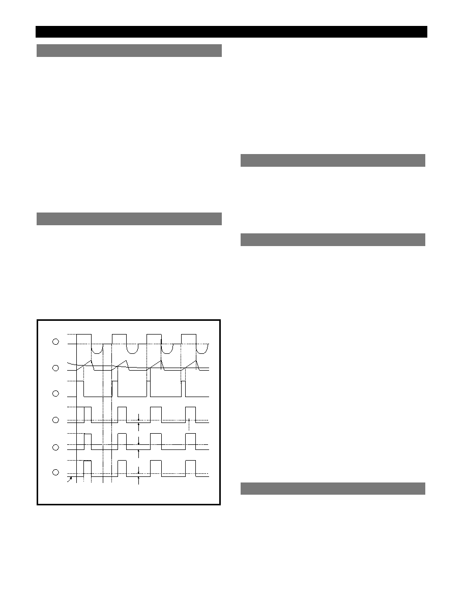
The SYNC circuit is activated at time t1 (Figure 1) when
the voltage at the SYNC pin exceeds the threshold level
(2.5V) of the SYNC comparator. The external ramp capac-
itor CR is allowed to charge through the internal current
source I (200A). At time t2, the ramp voltage intersects
with the control voltage VC and the output of the PWM
comparator goes high, turning on the output stage and
the external power switch. At the same time, the PWM
comparator is latched by the RS latch, LATCH.
Figure 1. Waveforms for CS5101. The number to the left of each curve
refers to a node on the Application Diagram.
The logic state of the LATCH can be changed only when
both the voltage level of the trailing edge of the power
pulse at the SYNC pin is less than the threshold voltage of
the SYNC comparator (2.5V) and the RAMP voltage is
less than the threshold voltage of the RAMP comparator
(1.65V). On the negative going transition of the secondary
side pulse VSY, gate G2 output goes high, resetting the
latch at time t3. Capacitor CR is discharged through tran-
sistor Q4. CR’s output goes low disabling the output stage,
and the external power switch (an N-FET) is turned off.
The value of the ramp capacitor CR is based on the
switching frequency of the regulator and the maximum
duty cycle of the secondary pulse VSY.
If the RAMP pin is pulled externally to 0.3V or below, the
SSPR is disabled. Current drawn by the IC is reduced to
less than 100A, and the IC is in SLEEP mode.
The voltage at the VCC pin is monitored by the undervolt-
age lockout comparator with hysteresis. When VCC falls
below the UVL threshold, the 5V reference and all the cir-
cuitry running off of it is disabled. Under this condition
the supply current is reduced to less than 500A.
The VCC supply voltage is further monitored by the
VCC_OK comparator. When VCC is reduced below
VREF - 0.7V, a fault signal is sent to gate G1. This fault sig-
nal, which determines if VCC is absent, works in conjunc-
tion with the ramp signal to disable the output, but only
after the current cycle has finished and the RS latch is reset.
Therefore this fault will not cause the output to turn off
during the middle of an on pulse, but rather will utilize
lossless turn-off. This feature protects the FET from over-
voltage stress. This is accomplished through gate G1 by
driving transistor Q4 on.
An additional fault signal is derived from the REF_OK
comparator. VREF is monitored so to disable the output
through gate G1 when the VREF voltage falls below the
OK threshold. As in the VCC_OK fault, the REF_OK fault
disables the output after the current cycle has been com-
pleted. The fault logic will operate normally only when
VREF voltage is within the specification limits of REF_OK.
The drain pin, VD monitors the voltage on the drain of the
power switch and derives energy from it to keep the out-
put stage in an off state when VC or VCC is below the min-
imum specified voltage.
DRAIN Function
FAULT Function
RAMP Function
0V
VSY
VSY + VD
VSY
0V
VSY – VOUT
0V
VSY + VC
t1 t2 t3
t4
t1
VD
VOUT + VD
VD
VG
VL1
VS
VDS
VC
VRAMP
VSY
1
2
3
4
5
6
Ground Level
(Gate doesn't go
below Gnd)
SYNC Function
Theory of Operation
相关PDF资料 |
PDF描述 |
|---|---|
| CS5101EDW16 | 1.5 A SWITCHING CONTROLLER, PDSO16 |
| CS5132HGDWR24 | 1.5 A DUAL SWITCHING CONTROLLER, PDSO24 |
| CS5151HGDR16 | 1.5 A SWITCHING CONTROLLER, 1000 kHz SWITCHING FREQ-MAX, PDSO16 |
| CS5158GD16 | 1.5 A SWITCHING CONTROLLER, 1000 kHz SWITCHING FREQ-MAX, PDSO16 |
| CS52845ED14 | 1 A SWITCHING CONTROLLER, PDSO14 |
相关代理商/技术参数 |
参数描述 |
|---|---|
| CS5101EN14G | 功能描述:初级与次级侧 PWM 控制器 Secondary Side 1.5A PWM AC/DC and DC/DC RoHS:否 制造商:ON Semiconductor 输出端数量:1 开关频率:250 KHz 工作电源电压:- 0.3 V to + 28 V 最大工作温度:+ 85 C 最小工作温度:- 5 C 封装 / 箱体:SOIC-8 Narrow 封装:Reel |
| CS5101-JL16 | 制造商:未知厂家 制造商全称:未知厂家 功能描述:Single-Ended Data Acquisition System |
| CS5101-JL8 | 制造商:未知厂家 制造商全称:未知厂家 功能描述:Single-Ended Data Acquisition System |
| CS5101-JP16 | 制造商:未知厂家 制造商全称:未知厂家 功能描述:Single-Ended Data Acquisition System |
| CS5101-JP8 | 制造商:未知厂家 制造商全称:未知厂家 功能描述:Single-Ended Data Acquisition System |
发布紧急采购,3分钟左右您将得到回复。