- 您现在的位置:买卖IC网 > PDF目录17351 > CS51411EVB (ON Semiconductor)EVAL BOARD FOR CS51411 HI FREQ PDF资料下载
参数资料
| 型号: | CS51411EVB |
| 厂商: | ON Semiconductor |
| 文件页数: | 11/20页 |
| 文件大小: | 0K |
| 描述: | EVAL BOARD FOR CS51411 HI FREQ |
| 设计资源: | CS51411EVB BOM CS51411EVB Gerber Files CS51411 Demo Brd Schematic |
| 标准包装: | 1 |
| 主要目的: | DC/DC,步降 |
| 输出及类型: | 1,非隔离 |
| 输出电压: | 3.3V |
| 电流 - 输出: | 1.5A |
| 输入电压: | 4 ~ 16 V |
| 稳压器拓扑结构: | 降压 |
| 频率 - 开关: | 260kHz |
| 板类型: | 完全填充 |
| 已供物品: | 板 |
| 已用 IC / 零件: | CS51411 |
| 其它名称: | CS51411EVBOS |
�� �
�
�CS51411,� CS51412,� CS51413,� CS51414�
�V� IN�
�Q2�
�where:�
�V� C� =� V� C� pin� steady� ?� state� voltage,� which� is� approximately�
�equal� to� error� amplifier� ’s� reference� voltage.�
�I1�
� � 5� m� A�
�To� internal�
�bias� rails�
�C� COMP� =� Compensation� capacitor� connected� to� the� V� C� pin�
�I� SOURCE� =� Output� Source� Current� of� the� error� amplifier.�
�SHDNB�
�(a)�
�20k�
�D1�
�8V�
�Q1�
�0.65V�
�Using� a� 0.1� m� F� C� COMP� ,� the� calculation� shows� a� T� SS� over�
�5.0� ms� which� is� adequate� to� avoid� any� current� stresses.�
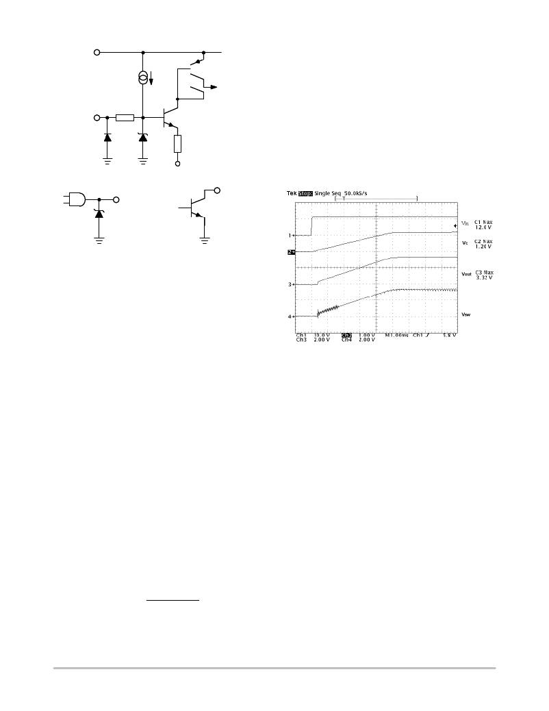
�Figure� 16� shows� the� gradual� rise� of� the� V� C� ,� V� O� and� envelope�
�of� the� V� SW� during� power� up.� There� is� no� voltage� overshoot�
�after� the� output� voltage� reaches� the� regulation.� If� the� supply�
�voltage� rises� slower� than� the� V� C� pin,� output� voltage� may�
�overshoot.�
�SHDNB�
�SHDNB�
�Z1�
�(b)�
�2V� to� 5V�
�(c)�
�Figure� 15.� SHDNB� pin� equivalent� internal� circuit� (a)�
�and� practical� interface� examples� (b),� (c).�
�Figure� 15(a)� depicts� the� SHDNB� pin� equivalent� internal�
�circuit.� If� the� pin� is� open,� current� source� I1� flows� into� the�
�base� of� Q1,� turning� both� Q1� and� Q2� on.� In� turn,� Q2� collector�
�current� enables� the� various� internal� power� rails.� In�
�Figure� 15(b),� a� standard� logic� gate� is� used� to� pull� the� pin� low�
�by� shunting� I1� to� ground,� which� places� the� IC� in� sleep�
�TSS� +� C�
�(shutdown)� mode.� Note� that,� when� the� gate� output� is� logical�
�high,� the� voltage� at� the� SHDNB� pin� will� rise� to� the� internal�
�clamp� voltage� of� 8� V.� This� level� exceeds� the� maximum�
�output� rating� for� most� common� logic� families.� Protection�
�Zener� diode� Z1� permits� the� pin� voltage� to� rise� high� enough�
�to� enable� the� IC,� but� remain� less� than� the� gate� output� voltage�
�rating.� In� Figure� 15(c),� a� single� open-collector� general-�
�purpose� NPN� transistor� is� used� to� pull� the� pin� low.� Since�
�transistors� generally� have� a� maximum� collector� voltage�
�rating� in� excess� of� 8� V,� the� protection� Zener� diode� in�
�Figure� 15(b)� is� not� required.�
�Startup�
�During� power� up,� the� regulator� tends� to� quickly� charge� up�
�the� output� capacitors� to� reach� voltage� regulation.� This� gives�
�rise� to� an� excessive� in� ?� rush� current� which� can� be� detrimental�
�to� the� inductor,� IC� and� catch� diode.� In� V� 2� control,� the�
�compensation� capacitor� provides� Soft� ?� Start� with� no� need�
�for� extra� pin� or� circuitry.� During� the� power� up,� the� Output�
�Source� Current� of� the� error� amplifier� charges� the�
�compensation� capacitor� which� forces� V� C� pin� and� thus� output�
�voltage� ramp� up� gradually.�
�The� Soft� ?� Start� duration� can� be� calculated� by�
�V CCOMP�
�ISOURCE�
�Figure� 16.� The� Power� Up� Transition� of� CS5141X�
�Regulator�
�Short� Circuit�
�When� the� V� FB� pin� voltage� drops� below� Foldback�
�Threshold,� the� regulator� reduces� the� peak� current� limit� by�
�40%� and� switching� frequency� to� 1/4� of� the� nominal�
�frequency.� These� features� are� designed� to� protect� the� IC� and�
�external� components� during� overload� or� short� circuit�
�conditions.� In� those� conditions,� peak� switching� current� is�
�clamped� to� the� current� limit� threshold.� The� reduced�
�switching� frequency� significantly� increases� the� ripple�
�current,� and� thus� lowers� the� DC� current.� The� short� circuit� can�
�cause� the� minimum� duty� cycle� to� be� limited� by� Minimum�
�Output� Pulse� Width.� The� foldback� frequency� reduces� the�
�minimum� duty� cycle� by� extending� the� switching� cycle.� This�
�protects� the� IC� from� overheating,� and� also� limits� the� power�
�that� can� be� transferred� to� the� output.� The� current� limit�
�foldback� effectively� reduces� the� current� stress� on� the�
�inductor� and� diode.� When� the� output� is� shorted,� the� DC�
�current� of� the� inductor� and� diode� can� approach� the� current�
�limit� threshold.� Therefore,� reducing� the� current� limit� by� 40%�
�can� result� in� an� equal� percentage� drop� of� the� inductor� and�
�diode� current.� The� short� circuit� waveforms� are� captured� in�
�http://onsemi.com�
�11�
�相关PDF资料 |
PDF描述 |
|---|---|
| RBM06DCWD | CONN EDGECARD 12POS DIP .156 SLD |
| A9BAG-1604F | FLEX CABLE - AFF16G/AF16/AFE16T |
| TARQ224K035 | CAP TANT 0.22UF 35V 10% AXIAL |
| A9BAA-0502E | FLEX CABLE - AFJ05A/AE05/AFH05T |
| AS1329A EB | BOARD EVAL AS1329A |
相关代理商/技术参数 |
参数描述 |
|---|---|
| CS51411GD8 | 功能描述:直流/直流开关调节器 1.5A Low Voltage RoHS:否 制造商:International Rectifier 最大输入电压:21 V 开关频率:1.5 MHz 输出电压:0.5 V to 0.86 V 输出电流:4 A 输出端数量: 最大工作温度: 安装风格:SMD/SMT 封装 / 箱体:PQFN 4 x 5 |
| CS51411GD8G | 功能描述:直流/直流开关调节器 1.5A Low Voltage Buck RoHS:否 制造商:International Rectifier 最大输入电压:21 V 开关频率:1.5 MHz 输出电压:0.5 V to 0.86 V 输出电流:4 A 输出端数量: 最大工作温度: 安装风格:SMD/SMT 封装 / 箱体:PQFN 4 x 5 |
| CS51411GDR8 | 功能描述:直流/直流开关调节器 1.5A Low Voltage RoHS:否 制造商:International Rectifier 最大输入电压:21 V 开关频率:1.5 MHz 输出电压:0.5 V to 0.86 V 输出电流:4 A 输出端数量: 最大工作温度: 安装风格:SMD/SMT 封装 / 箱体:PQFN 4 x 5 |
| CS51411GDR8G | 功能描述:直流/直流开关调节器 1.5A Low Voltage Buck RoHS:否 制造商:International Rectifier 最大输入电压:21 V 开关频率:1.5 MHz 输出电压:0.5 V to 0.86 V 输出电流:4 A 输出端数量: 最大工作温度: 安装风格:SMD/SMT 封装 / 箱体:PQFN 4 x 5 |
| CS51411GMNR2G | 功能描述:直流/直流开关调节器 BUCK REGULATOR RoHS:否 制造商:International Rectifier 最大输入电压:21 V 开关频率:1.5 MHz 输出电压:0.5 V to 0.86 V 输出电流:4 A 输出端数量: 最大工作温度: 安装风格:SMD/SMT 封装 / 箱体:PQFN 4 x 5 |
发布紧急采购,3分钟左右您将得到回复。