- 您现在的位置:买卖IC网 > PDF目录17351 > CS51411EVB (ON Semiconductor)EVAL BOARD FOR CS51411 HI FREQ PDF资料下载
参数资料
| 型号: | CS51411EVB |
| 厂商: | ON Semiconductor |
| 文件页数: | 8/20页 |
| 文件大小: | 0K |
| 描述: | EVAL BOARD FOR CS51411 HI FREQ |
| 设计资源: | CS51411EVB BOM CS51411EVB Gerber Files CS51411 Demo Brd Schematic |
| 标准包装: | 1 |
| 主要目的: | DC/DC,步降 |
| 输出及类型: | 1,非隔离 |
| 输出电压: | 3.3V |
| 电流 - 输出: | 1.5A |
| 输入电压: | 4 ~ 16 V |
| 稳压器拓扑结构: | 降压 |
| 频率 - 开关: | 260kHz |
| 板类型: | 完全填充 |
| 已供物品: | 板 |
| 已用 IC / 零件: | CS51411 |
| 其它名称: | CS51411EVBOS |
�� �
�
�CS51411,� CS51412,� CS51413,� CS51414�
�Control� Ramp� Generation�
�In� original� V2� designs,� the� control� ramp� VCR� was�
�generated� from� the� converter’s� output� ripple.� Using� a� current�
�derived� ramp� provides� the� same� benefits� as� current� mode,�
�V� IN�
�R�
�C�
�V� OUT�
�namely� input� feed� forward,� single� pole� output� filter�
�compensation� and� fast� feedback� following� output� load�
�transients.� Typically� a� tantalum� or� organic� polymer�
�capacitor� is� selected� having� a� sufficiently� large� ESR�
�component,� relative� to� its� capacitive� and� ESL� ripple�
�contributions,� to� ensure� the� control� ramp� was� sensing�
�inductor� current� and� its� amplitude� was� sufficient� to� maintain�
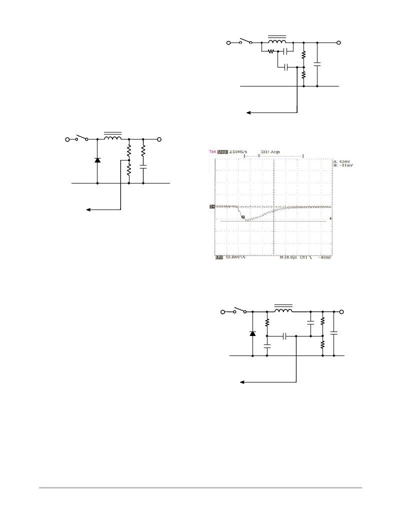
�loop� stability.� This� technique� is� illustrated� in� Figure� 6.�
�V� FB�
�Figure� 7.� Control� Ramp� Generated� from� DCR�
�V� IN�
�L�
�C� esr�
�V� OUT�
�Inductor� Sensing�
�C�
�V� FB�
�Figure� 6.� Control� Ramp� Generated� from� Output�
�Advances� in� multilayer� ceramic� capacitor� technology� are�
�such� that� MLCC’s� can� provide� a� cost� effective� filter� solution�
�for� low� voltage� (<� 12� V),� high� frequency� converters�
�(>200� kHz).� For� example,� a� 10� m� F� MLCC� 16� V� in� a�
�805� SMT� package� has� an� ESR� of� 2� m� W� and� an� ESL� of�
�100� nH.� Using� several� MLCC’s� in� parallel,� connected� to�
�power� and� ground� planes� on� a� PCB� with� multiple� vias,� can�
�provide� a� “near� perfect”� capacitor.� Using� this� technique,�
�output� switching� ripple� below� 10� mV� can� be� readily�
�Figure� 8.�
�Ramp� generation� using� a� voltage� feed� forward� technique�
�is� illustrated� in� Figure� 9.�
�obtained� since� parasitic� ESR� and� ESL� ripple� contributions�
�are� nil.� In� this� case,� the� control� ramp� is� generated� elsewhere�
�in� the� circuit.�
�V� IN�
�R� f�
�C� Z�
�V� OUT�
�Ramp� generation� using� dcr� inductor� current� sensing,�
�where� the� L/DCR� time� constant� of� the� output� inductor� is�
�matched� with� the� CR� time� constant� of� the� integrating�
�network,� is� shown� in� Figure� 7.� The� converter� ’s� transient�
�response� following� a� 1� A� step� load� is� shown� in� Figure� 8.� This�
�transient� response� is� indicative� of� a� closed� loop� in� excess� of�
�10� kHz� having� good� gain� and� phase� margin� in� the� frequency�
�domain.� Also� note� the� amplitude� of� output� switching� ripple�
�provided� by� just� two� 10� m� F� MLCC’s.�
�C� f�
�V� FB�
�Figure� 9.� Control� Ramp� from� Voltage� Feed� Forward�
�http://onsemi.com�
�8�
�相关PDF资料 |
PDF描述 |
|---|---|
| RBM06DCWD | CONN EDGECARD 12POS DIP .156 SLD |
| A9BAG-1604F | FLEX CABLE - AFF16G/AF16/AFE16T |
| TARQ224K035 | CAP TANT 0.22UF 35V 10% AXIAL |
| A9BAA-0502E | FLEX CABLE - AFJ05A/AE05/AFH05T |
| AS1329A EB | BOARD EVAL AS1329A |
相关代理商/技术参数 |
参数描述 |
|---|---|
| CS51411GD8 | 功能描述:直流/直流开关调节器 1.5A Low Voltage RoHS:否 制造商:International Rectifier 最大输入电压:21 V 开关频率:1.5 MHz 输出电压:0.5 V to 0.86 V 输出电流:4 A 输出端数量: 最大工作温度: 安装风格:SMD/SMT 封装 / 箱体:PQFN 4 x 5 |
| CS51411GD8G | 功能描述:直流/直流开关调节器 1.5A Low Voltage Buck RoHS:否 制造商:International Rectifier 最大输入电压:21 V 开关频率:1.5 MHz 输出电压:0.5 V to 0.86 V 输出电流:4 A 输出端数量: 最大工作温度: 安装风格:SMD/SMT 封装 / 箱体:PQFN 4 x 5 |
| CS51411GDR8 | 功能描述:直流/直流开关调节器 1.5A Low Voltage RoHS:否 制造商:International Rectifier 最大输入电压:21 V 开关频率:1.5 MHz 输出电压:0.5 V to 0.86 V 输出电流:4 A 输出端数量: 最大工作温度: 安装风格:SMD/SMT 封装 / 箱体:PQFN 4 x 5 |
| CS51411GDR8G | 功能描述:直流/直流开关调节器 1.5A Low Voltage Buck RoHS:否 制造商:International Rectifier 最大输入电压:21 V 开关频率:1.5 MHz 输出电压:0.5 V to 0.86 V 输出电流:4 A 输出端数量: 最大工作温度: 安装风格:SMD/SMT 封装 / 箱体:PQFN 4 x 5 |
| CS51411GMNR2G | 功能描述:直流/直流开关调节器 BUCK REGULATOR RoHS:否 制造商:International Rectifier 最大输入电压:21 V 开关频率:1.5 MHz 输出电压:0.5 V to 0.86 V 输出电流:4 A 输出端数量: 最大工作温度: 安装风格:SMD/SMT 封装 / 箱体:PQFN 4 x 5 |
发布紧急采购,3分钟左右您将得到回复。