- 您现在的位置:买卖IC网 > PDF目录17333 > CS5171BSTGEVB (ON Semiconductor)EVAL BOARD FOR CS5171BST PDF资料下载
参数资料
| 型号: | CS5171BSTGEVB |
| 厂商: | ON Semiconductor |
| 文件页数: | 17/21页 |
| 文件大小: | 0K |
| 描述: | EVAL BOARD FOR CS5171BST |
| 设计资源: | CS5171BSTGEVB Gerber Files |
| 标准包装: | 1 |
| 主要目的: | DC/DC,步升 |
| 输出及类型: | 1,非隔离 |
| 输出电压: | 5V |
| 电流 - 输出: | 400mA |
| 输入电压: | 3.3V |
| 稳压器拓扑结构: | 升压 |
| 频率 - 开关: | 260kHz |
| 板类型: | 完全填充 |
| 已供物品: | 板 |
| 已用 IC / 零件: | CS5171 |
| 其它名称: | CS5171BSTEVBOS CS5171BSTEVBOS-ND CS5171BSTGEVBOS |
�� �
�
�CS5171,� CS5172,� CS5173,� CS5174�
�TJ� +� TA� )� (PD� q� JA)�
�where:�
�transitions� that� can� cause� problems.� Therefore� the� following�
�guidelines� should� be� followed� in� the� layout.�
�T� J� =� IC� or� FET� junction� temperature� (� °� C);�
�T� A� =� ambient� temperature� (� °� C);�
�P� D� =� power� dissipated� by� part� in� question� (W);�
�q� JA� =� junction� ?� to� ?� ambient� thermal� resistance� (� °� C/W).�
�For� the� CS517x,� q� JA� =165� °� C/W.�
�Once� the� designer� has� calculated� T� J� ,� the� question� of�
�whether� the� CS517x� can� be� used� in� an� application� is� settled.�
�If� T� J� exceeds� 150� °� C,� the� absolute� maximum� allowable�
�junction� temperature,� the� CS517x� is� not� suitable� for� that�
�application.�
�If� T� J� approaches� 150� °� C,� the� designer� should� consider�
�possible� means� of� reducing� the� junction� temperature.�
�Perhaps� another� converter� topology� could� be� selected� to�
�reduce� the� switch� current.� Increasing� the� airflow� across� the�
�surface� of� the� chip� might� be� considered� to� reduce� T� A� .�
�Circuit� Layout� Guidelines�
�In� any� switching� power� supply,� circuit� layout� is� very�
�important� for� proper� operation.� Rapidly� switching� currents�
�combined� with� trace� inductance� generates� voltage�
�1.�
�2.�
�3.�
�In� boost� circuits,� high� AC� current� circulates� within� the�
�loop� composed� of� the� diode,� output� capacitor,� and�
�on� ?� chip� power� transistor.� The� length� of� associated�
�traces� and� leads� should� be� kept� as� short� as� possible.� In�
�the� flyback� circuit,� high� AC� current� loops� exist� on� both�
�sides� of� the� transformer.� On� the� primary� side,� the� loop�
�consists� of� the� input� capacitor,� transformer,� and�
�on� ?� chip� power� transistor,� while� the� transformer,�
�rectifier� diodes,� and� output� capacitors� form� another�
�loop� on� the� secondary� side.� Just� as� in� the� boost� circuit,�
�all� traces� and� leads� containing� large� AC� currents�
�should� be� kept� short.�
�Separate� the� low� current� signal� grounds� from� the�
�power� grounds.� Use� single� point� grounding� or� ground�
�plane� construction� for� the� best� results.�
�Locate� the� voltage� feedback� resistors� as� near� the� IC� as�
�possible� to� keep� the� sensitive� feedback� wiring� short.�
�Connect� feedback� resistors� to� the� low� current� analog�
�ground.�
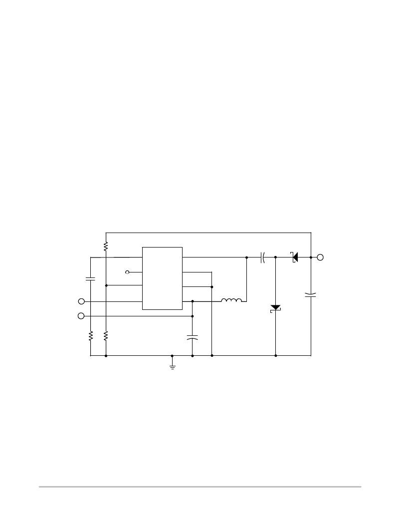
�C1�
�R2�
�4.87� k�
�1�
�2�
�V� C�
�Test�
�V� SW�
�PGND�
�8�
�7�
�C4�
�+�
�22� m� F�
�D1�
�MBRS120T3�
�V� OUT�
�?� 12� V�
�SS�
�0.01� m� F�
�SS�
�V� CC�
�5.0� V�
�3� NFB�
�4�
�AGND�
�V� CC�
�6�
�5�
�L1�
�22� m� H�
�D2�
�MBRS120T3�
�+�
�C3�
�22� m� F�
�R1�
�5.0� k�
�R3�
�1.27� k�
�+�
�C2�
�22� m� F�
�Figure� 41.� Additional� Application� Diagram,� 5.0� V� to� ?� 12� V/� 75� mA� Inverting� Converter�
�http://onsemi.com�
�17�
�相关PDF资料 |
PDF描述 |
|---|---|
| HK100568NJ-T | INDUCTOR HI FREQ 68NH 5% 0402 |
| F930G477MNC | CAP TANT 470UF 4V 20% 2917 |
| ASPI-0630HI-1R0M-T15 | INDUCTOR POWER 1.0UH 0630 SMD |
| HK10055N1S-T | INDUCTOR HIFREQ 5.1+/-0.3NH 0402 |
| ISL8204MEVAL1Z | EVAL BOARD 1 FOR ISL8204 |
相关代理商/技术参数 |
参数描述 |
|---|---|
| CS5171ED8 | 功能描述:直流/直流开关调节器 1.5A High Efficiency RoHS:否 制造商:International Rectifier 最大输入电压:21 V 开关频率:1.5 MHz 输出电压:0.5 V to 0.86 V 输出电流:4 A 输出端数量: 最大工作温度: 安装风格:SMD/SMT 封装 / 箱体:PQFN 4 x 5 |
| CS5171ED8G | 功能描述:直流/直流开关调节器 1.5A High Efficiency Boost RoHS:否 制造商:International Rectifier 最大输入电压:21 V 开关频率:1.5 MHz 输出电压:0.5 V to 0.86 V 输出电流:4 A 输出端数量: 最大工作温度: 安装风格:SMD/SMT 封装 / 箱体:PQFN 4 x 5 |
| CS5171EDR8 | 功能描述:直流/直流开关调节器 1.5A High Efficiency RoHS:否 制造商:International Rectifier 最大输入电压:21 V 开关频率:1.5 MHz 输出电压:0.5 V to 0.86 V 输出电流:4 A 输出端数量: 最大工作温度: 安装风格:SMD/SMT 封装 / 箱体:PQFN 4 x 5 |
| CS5171EDR8G | 功能描述:直流/直流开关调节器 1.5A High Efficiency Boost RoHS:否 制造商:International Rectifier 最大输入电压:21 V 开关频率:1.5 MHz 输出电压:0.5 V to 0.86 V 输出电流:4 A 输出端数量: 最大工作温度: 安装风格:SMD/SMT 封装 / 箱体:PQFN 4 x 5 |
| CS5171GD8 | 功能描述:直流/直流开关调节器 1.5A High Efficiency RoHS:否 制造商:International Rectifier 最大输入电压:21 V 开关频率:1.5 MHz 输出电压:0.5 V to 0.86 V 输出电流:4 A 输出端数量: 最大工作温度: 安装风格:SMD/SMT 封装 / 箱体:PQFN 4 x 5 |
发布紧急采购,3分钟左右您将得到回复。