- 您现在的位置:买卖IC网 > PDF目录13377 > CS5171EDR8 (ON Semiconductor)IC REG MULTI CONFIG 1.5A 8SOIC PDF资料下载
参数资料
| 型号: | CS5171EDR8 |
| 厂商: | ON Semiconductor |
| 文件页数: | 12/21页 |
| 文件大小: | 0K |
| 描述: | IC REG MULTI CONFIG 1.5A 8SOIC |
| 产品变化通告: | Product Discontinuation 27/Jun/2007 |
| 标准包装: | 1 |
| 类型: | 升压(升压),回扫,正向转换器,Sepic |
| 输出数: | 1 |
| 输入电压: | 2.7 V ~ 30 V |
| PWM 型: | 电流模式 |
| 频率 - 开关: | 280kHz |
| 电流 - 输出: | 1.5A |
| 同步整流器: | 无 |
| 工作温度: | -40°C ~ 85°C |
| 安装类型: | 表面贴装 |
| 封装/外壳: | 8-SOIC(0.154",3.90mm 宽) |
| 包装: | 剪切带 (CT) |
| 供应商设备封装: | 8-SOICN |
| 其它名称: | CS5171EDR8OSCT |
�� �
�
�CS5171,� CS5172,� CS5173,� CS5174�
�fZ1� +�
�The� first� zero� generated� by� C1� and� R1� is:�
�1�
�2� p� C1R1�
�The� phase� lead� provided� by� this� zero� ensures� that� the� loop�
�?� V� OUT�
�R1�
�2V�
�R� P�
�200� k� W�
�fP� +�
�has� at� least� a� 45� °� phase� margin� at� the� crossover� frequency.�
�Therefore,� this� zero� should� be� placed� close� to� the� pole�
�generated� in� the� power� stage� which� can� be� identified� at�
�frequency:�
�1�
�2� p� CORLOAD�
�R2�
�NFB�
�R� IN�
�250� k� W�
�+�
�?�
�Negative� Error� ?� Amp�
�fP2� +�
�*� (15� m� A�
�R1)� v� VOFFSET�
�*� (5� m� A�
�0.0.5� (R1� )� R2)�
�R2�
�where:�
�C� O� =� equivalent� output� capacitance� of� the� error� amplifier�
�≈� 120pF;�
�R� LOAD� =� load� resistance.�
�The� high� frequency� pole,� f� P2� ,� can� be� placed� at� the� output�
�filter� ’s� ESR� zero� or� at� half� the� switching� frequency.� Placing�
�the� pole� at� this� frequency� will� cut� down� on� switching� noise.�
�The� frequency� of� this� pole� is� determined� by� the� value� of� C2�
�and� R1:�
�1�
�2� p� C2R1�
�One� simple� method� to� ensure� adequate� phase� margin� is� to�
�design� the� frequency� response� with� a� ?� 20� dB� per� decade�
�slope,� until� unity� ?� gain� crossover.� The� crossover� frequency�
�should� be� selected� at� the� midpoint� between� f� Z1� and� f� P2� where�
�the� phase� margin� is� maximized.�
�f� P1�
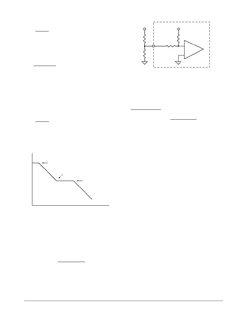
�Figure� 33.� Negative� Error� Amplifier� and� NFB� Pin�
�It� is� shown� that� if� R1� is� less� than� 10� k,� the� deviation� from�
�the� design� target� will� be� less� than� 0.1� V.� If� the� tolerances� of�
�the� negative� voltage� reference� and� NFB� pin� input� current� are�
�considered,� the� possible� offset� of� the� output� V� OFFSET� varies�
�in� the� range� of:�
�*� 0.0.5 (R1� )� R2)�
�R2�
�v� R1)�
�V� SW� Voltage� Limit�
�In� the� boost� topology,� V� SW� pin� maximum� voltage� is� set� by�
�the� maximum� output� voltage� plus� the� output� diode� forward�
�voltage.� The� diode� forward� voltage� is� typically� 0.5� V� for�
�Schottky� diodes� and� 0.8� V� for� ultrafast� recovery� diodes�
�VSW(MAX)� +� VOUT(MAX)� )� VF�
�f� Z1�
�f� P2�
�where:�
�V� F� =� output� diode� forward� voltage.�
�In� the� flyback� topology,� peak� V� SW� voltage� is� governed� by:�
�VSW(MAX)� +� VCC(MAX)� )� (VOUT� )� VF)�
�N�
�where:�
�N� =� transformer� turns� ratio,� primary� over� secondary.�
�Frequency� (LOG)�
�Figure� 32.� Bode� Plot� of� the� Compensation� Network�
�Shown� in� Figure� 31�
�Negative� Voltage� Feedback�
�Since� the� negative� error� amplifier� has� finite� input�
�impedance� as� shown� in� Figure� 33,� its� induced� error� has� to� be�
�considered.� If� a� voltage� divider� is� used� to� scale� down� the�
�negative� output� voltage� for� the� NFB� pin,� the� equation� for�
�calculating� output� voltage� is:�
�When� the� power� switch� turns� off,� there� exists� a� voltage�
�spike� superimposed� on� top� of� the� steady� ?� state� voltage.�
�Usually� this� voltage� spike� is� caused� by� transformer� leakage�
�inductance� charging� stray� capacitance� between� the� V� SW� and�
�PGND� pins.� To� prevent� the� voltage� at� the� V� SW� pin� from�
�exceeding� the� maximum� rating,� a� transient� voltage�
�suppressor� in� series� with� a� diode� is� paralleled� with� the�
�primary� windings.� Another� method� of� clamping� switch�
�voltage� is� to� connect� a� transient� voltage� suppressor� between�
�the� V� SW� pin� and� ground.�
�*� VOUT� +�
�*� 2.5 (R1� )� R2)�
�R2�
�*� 10� m� A�
�R1�
�http://onsemi.com�
�12�
�相关PDF资料 |
PDF描述 |
|---|---|
| VI-20T-EX-F1 | CONVERTER MOD DC/DC 6.5V 75W |
| VE-J6K-EY-F1 | CONVERTER MOD DC/DC 40V 50W |
| RSC20DRTN-S734 | CONN EDGECARD 40POS DIP .100 SLD |
| VI-20L-EX-F1 | CONVERTER MOD DC/DC 28V 75W |
| VE-J6J-EY-F2 | CONVERTER MOD DC/DC 36V 50W |
相关代理商/技术参数 |
参数描述 |
|---|---|
| CS5171EDR8G | 功能描述:直流/直流开关调节器 1.5A High Efficiency Boost RoHS:否 制造商:International Rectifier 最大输入电压:21 V 开关频率:1.5 MHz 输出电压:0.5 V to 0.86 V 输出电流:4 A 输出端数量: 最大工作温度: 安装风格:SMD/SMT 封装 / 箱体:PQFN 4 x 5 |
| CS5171GD8 | 功能描述:直流/直流开关调节器 1.5A High Efficiency RoHS:否 制造商:International Rectifier 最大输入电压:21 V 开关频率:1.5 MHz 输出电压:0.5 V to 0.86 V 输出电流:4 A 输出端数量: 最大工作温度: 安装风格:SMD/SMT 封装 / 箱体:PQFN 4 x 5 |
| CS5171GD8G | 功能描述:直流/直流开关调节器 1.5A High Efficiency Boost RoHS:否 制造商:International Rectifier 最大输入电压:21 V 开关频率:1.5 MHz 输出电压:0.5 V to 0.86 V 输出电流:4 A 输出端数量: 最大工作温度: 安装风格:SMD/SMT 封装 / 箱体:PQFN 4 x 5 |
| CS5171GDR8 | 功能描述:直流/直流开关调节器 1.5A High Efficiency RoHS:否 制造商:International Rectifier 最大输入电压:21 V 开关频率:1.5 MHz 输出电压:0.5 V to 0.86 V 输出电流:4 A 输出端数量: 最大工作温度: 安装风格:SMD/SMT 封装 / 箱体:PQFN 4 x 5 |
| CS5171GDR8G | 功能描述:直流/直流开关调节器 1.5A High Efficiency Boost RoHS:否 制造商:International Rectifier 最大输入电压:21 V 开关频率:1.5 MHz 输出电压:0.5 V to 0.86 V 输出电流:4 A 输出端数量: 最大工作温度: 安装风格:SMD/SMT 封装 / 箱体:PQFN 4 x 5 |
发布紧急采购,3分钟左右您将得到回复。