- 您现在的位置:买卖IC网 > PDF目录298969 > CS5208-1GT3 1.25 V-5 V ADJUSTABLE POSITIVE LDO REGULATOR, 1.3 V DROPOUT, PSFM3 PDF资料下载
参数资料
| 型号: | CS5208-1GT3 |
| 元件分类: | 可调正电压单路输出LDO稳压器 |
| 英文描述: | 1.25 V-5 V ADJUSTABLE POSITIVE LDO REGULATOR, 1.3 V DROPOUT, PSFM3 |
| 封装: | STRAIGHT, TO-220, 3 PIN |
| 文件页数: | 5/7页 |
| 文件大小: | 148K |
| 代理商: | CS5208-1GT3 |
CS5208-1
Application Notes: continued
5
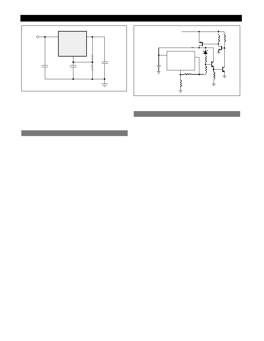
Figure 1.
While not required, a bypass capacitor connected between
the adjust pin and ground will improve transient response
and ripple rejection. A 0.1F tantalum capacitor is recom-
mended for “first cut” design. Value and type may be var-
ied to optimize performance vs price.
The CS5208-1 linear regulator has an absolute maximum
specification of 6V for the voltage difference between VIN
and VOUT. However, the IC may be used to regulate volt-
ages in excess of 6V. The main considerations in such a
design are power-up and short circuit capability.
In most applications, ramp-up of the power supply to VIN
is fairly slow, typically on the order of several tens of mil-
liseconds, while the regulator responds in less than one
microsecond. In this case, the linear regulator begins charg-
ing the output capacitor as soon as the VIN to VOUT differ-
ential is large enough that the pass transistor conducts cur-
rent. VOUT is essentially at ground, and VIN is on the order
of several hundred millivolts, so the pass transistor is in
dropout. As VIN increases, the pass transistor will remain
in dropout, and current is passed to the load until VOUT is
in regulation. Further increase in VIN brings the pass tran-
sistor out of dropout. The result is that the output voltage
follows the power supply ramp-up, staying in dropout
until the regulation point is reached. In this manner, any
output voltage may be regulated. There is no theoretical
limit to the regulated voltage as long as the VIN to VOUT
differential of 6V is not exceeded.
However, the maximum ratings of the IC will be exceeded
in a short circuit condition. Short circuit conditions will
result in the immediate operation of the pass transistor
outside of its safe operating area. Over-voltage stresses will
then cause destruction of the pass transistor before over-
current or thermal shutdown circuitry can become active.
Additional circuitry may be required to clamp VIN to VOUT
differential to less than 6V if failsafe operation is required.
One possible clamp circuit is illustrated below; however,
the design of clamp circuitry must be done on an applica-
tion by application basis. Care must be taken to ensure the
clamp actually protects the design. Components used in
the clamp design must be able to withstand the short cir-
cuit conditions indefinitely while protecting the IC.
Figure 2.
The output compensation capacitor helps determine three
main characteristics of a linear regulator: start-up delay,
load transient response, and loop stability.
The capacitor value and type is based on cost, availability,
size and temperature constraints. A tantalum or aluminum
electrolytic capacitor is best, since a film or ceramic capaci-
tor with almost zero ESR can cause instability. The alu-
minum electrolytic capacitor is the least expensive solu-
tion. However, when the circuit operates at low tempera-
tures, both the value and ESR of the capacitor will vary
considerably. The capacitor manufacturer’s data sheet pro-
vides this information.
A 300F tantalum capacitor will work for most applica-
tions, but with high current regulators such as the
CS5208-1 the transient response and stability improve with
higher values of capacitance. The majority of applications
for this regulator involve large changes in load
current so the output capacitor must supply the instanta-
neous load current. The ESR of the output capacitor causes
an immediate drop in output voltage given by:
V = I × ESR.
For microprocessor applications it is customary to use an
output capacitor network consisting of several tantalum
and ceramic capacitors in parallel. This reduces the overall
ESR and reduces the instantaneous output voltage drop
under transient load conditions. The output capacitor net-
work should be as close to the load as possible for the best
results.
Protection Diodes
When large external capacitors are used with a linear regu-
lator it is sometimes necessary to add protection diodes. If
the input voltage of the regulator gets shorted, the output
capacitor will discharge into the output of the regulator.
The discharge current depends on the value of the capaci-
tor, the output voltage, and the rate at which VIN drops. In
the CS5208-1 regulator, the discharge path is through a
large junction and protection diodes are not usually need-
ed. If the regulator is used with large values of output
capacitance and the input voltage is instantaneously short-
Stability Considerations
VIN
VOUT
VAdj
EXTERNAL SUPPLY
Other Adjustable Operation Considerations
V
OUT
V
IN
CS5208-1
R1
Adj
R2
相关PDF资料 |
PDF描述 |
|---|---|
| CS5411-4 | Optoelectronic |
| CS5411H4H | Optoelectronic |
| CS54123CP | 高速漏电保护开关电路 =M54123L |
| CS5412-AC1 | Analog-to-Digital Converter??? 12-Bit |
| CS5651GN16 | 0.4 A DUAL SWITCHING CONTROLLER, 500 kHz SWITCHING FREQ-MAX, PDIP16 |
相关代理商/技术参数 |
参数描述 |
|---|---|
| CS-5208-1T3 | 制造商:未知厂家 制造商全称:未知厂家 功能描述:Positive Adjustable Voltage Regulator |
| CS-5208A-1T3 | 制造商:未知厂家 制造商全称:未知厂家 功能描述:Positive Adjustable Voltage Regulator |
| CS5210-1 | 制造商:CHERRY 制造商全称:CHERRY 功能描述:10A LDO 3-Pin Adjustable Linear Regulator |
| CS5210-1/D | 制造商:未知厂家 制造商全称:未知厂家 功能描述:10A LDO 3-Pin Adjustable Linear RegulatorDescription |
| CS5210-1GT3 | 制造商:CHERRY 制造商全称:CHERRY 功能描述:10A LDO 3-Pin Adjustable Linear Regulator |
发布紧急采购,3分钟左右您将得到回复。