- 您现在的位置:买卖IC网 > PDF目录298969 > CS5208-1GT3 1.25 V-5 V ADJUSTABLE POSITIVE LDO REGULATOR, 1.3 V DROPOUT, PSFM3 PDF资料下载
参数资料
| 型号: | CS5208-1GT3 |
| 元件分类: | 可调正电压单路输出LDO稳压器 |
| 英文描述: | 1.25 V-5 V ADJUSTABLE POSITIVE LDO REGULATOR, 1.3 V DROPOUT, PSFM3 |
| 封装: | STRAIGHT, TO-220, 3 PIN |
| 文件页数: | 6/7页 |
| 文件大小: | 148K |
| 代理商: | CS5208-1GT3 |
6
CS5208-1
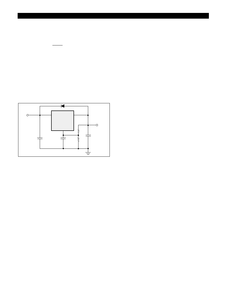
ed to ground, damage can occur. In this case, a diode con-
nected as shown in Figure 3 is recommended.
A rule of thumb useful in determining if a protection diode
is required is to solve for current
I =
, where
I is the current flow out of the load capacitance when
VIN is shorted,
C is the value of the load capacitance,
V is the output voltage, and
T is the time duration required for VIN to transition
from high to being shorted.
If the calculated current is greater than or equal to the typi-
cal short circuit current value provided in the specifica-
tions, serious thought should be given to including a pro-
tection diode.
Figure 3.
Current Limit
The internal current limit circuit limits the output current
under excessive load conditions and protects the regulator.
Short Circuit Protection
The device includes foldback short circuit current limit that
clamps the output current at approximately two amperes
less than its current limit value.
Thermal Shutdown
The thermal shutdown circuitry is guaranteed by design to
become activated above a die junction temperature of
150°C and to shut down the regulator output. This circuit-
ry includes a thermal hysteresis circuit with 25°C of typical
hysteresis, thereby allowing the regulator to recover from a
thermal fault automatically.
Calculating Power Dissipation and Heat Sink
Requirements
High power regulators such as the CS5208-1 usually oper-
ate at high junction temperatures. Therefore, it is important
to calculate the power dissipation and junction tempera-
tures accurately to ensure that an adequate heat sink is
used. Since the package tab is connected to Vout on the
CS5208-1, electrical isolation may be required for some
applications. Also, as with all high power packages, ther-
mal compound in necessary to ensure proper heat flow.
For added safety, this high current LDO includes an inter-
nal thermal shutdown circuit
The thermal characteristics of an IC depend on the follow-
ing four factors. Junction temperature, ambient tempera-
ture, die power dissipation, and the thermal resistance
from the die junction to ambient air. The maximum junc-
tion temperature can be determined by:
TJ(max) = TA(max) + PD(max) × RΘJA
The maximum ambient temperature and the power dissi-
pation are determined by the design while the maximum
junction temperature and the thermal resistance depend on
the manufacturer and the package type. The maximum
power dissipation for a regulator is:
PD(max) = (VIN(max) -VOUT(min))IOUT(max) + VIN(max) × IIN(max)
A heat sink effectively increases the surface area of the
package to improve the flow of heat away from the IC and
into the surrounding air. Each material in the heat flow
path between the IC and the outside environment has a
thermal resistance which is measured in degrees per watt.
Like series electrical resistances, these thermal resistances
are summed to determine the total thermal resistance
between the die junction and the surrounding air, RΘJA.
This total thermal resistance is comprised of three compo-
nents. These resistive terms are measured from junction to
case (RΘJC), case to heat sink (RΘCS), and heat sink to ambi-
ent air (RΘSA ). The equation is:
RΘJA = RΘJC + RΘCS + RΘSA
RΘJC is rated @ 1.4°C/W for the CS5208-1. For a high cur-
rent regulator such as the CS5208-1 the majority of heat is
generated in the power transistor section. The value for
RΘSA depends on the heat sink type, while the RΘCS
depends on factors such as package type, heat sink inter-
face (is an insulator and thermal grease used?), and the
contact area between the heat sink and the package. Once
these calculations are complete, the maximum permissible
value of RΘJA can be calculated and the proper heat sink
selected. For further discussion on heat sink selection, see
our Cherry application note “Thermal Management for
Linear Regulators.”
V
OUT
V
IN
CS5208-1
Adj
C × V
T
Application Notes: continued
相关PDF资料 |
PDF描述 |
|---|---|
| CS5411-4 | Optoelectronic |
| CS5411H4H | Optoelectronic |
| CS54123CP | 高速漏电保护开关电路 =M54123L |
| CS5412-AC1 | Analog-to-Digital Converter??? 12-Bit |
| CS5651GN16 | 0.4 A DUAL SWITCHING CONTROLLER, 500 kHz SWITCHING FREQ-MAX, PDIP16 |
相关代理商/技术参数 |
参数描述 |
|---|---|
| CS-5208-1T3 | 制造商:未知厂家 制造商全称:未知厂家 功能描述:Positive Adjustable Voltage Regulator |
| CS-5208A-1T3 | 制造商:未知厂家 制造商全称:未知厂家 功能描述:Positive Adjustable Voltage Regulator |
| CS5210-1 | 制造商:CHERRY 制造商全称:CHERRY 功能描述:10A LDO 3-Pin Adjustable Linear Regulator |
| CS5210-1/D | 制造商:未知厂家 制造商全称:未知厂家 功能描述:10A LDO 3-Pin Adjustable Linear RegulatorDescription |
| CS5210-1GT3 | 制造商:CHERRY 制造商全称:CHERRY 功能描述:10A LDO 3-Pin Adjustable Linear Regulator |
发布紧急采购,3分钟左右您将得到回复。