- 您现在的位置:买卖IC网 > PDF目录10250 > CS5532-BSZR (Cirrus Logic Inc)IC ADC 24BIT 2CH W/LNA 20-SSOP PDF资料下载
参数资料
| 型号: | CS5532-BSZR |
| 厂商: | Cirrus Logic Inc |
| 文件页数: | 16/17页 |
| 文件大小: | 0K |
| 描述: | IC ADC 24BIT 2CH W/LNA 20-SSOP |
| 标准包装: | 1,000 |
| 位数: | 24 |
| 采样率(每秒): | 3.84k |
| 数据接口: | 串行 |
| 转换器数目: | 1 |
| 功率耗散(最大): | 45mW |
| 电压电源: | 模拟和数字,双 ± |
| 工作温度: | -40°C ~ 85°C |
| 安装类型: | 表面贴装 |
| 封装/外壳: | 20-SSOP(0.209",5.30mm 宽) |
| 供应商设备封装: | 20-SSOP |
| 包装: | 带卷 (TR) |
| 输入数目和类型: | 2 个差分,单极;2 个差分,双极 |
| 配用: | 598-1159-ND - BOARD EVAL FOR CS5532U ADC |
IDT / ICS PCI EXPRESS JITTER ATTENUATOR
8
ICS9DB202CK-01 REV. B FEBRUARY 18, 2009
ICS9DB202-01
PCI EXPRESS JITTER ATTENUATOR
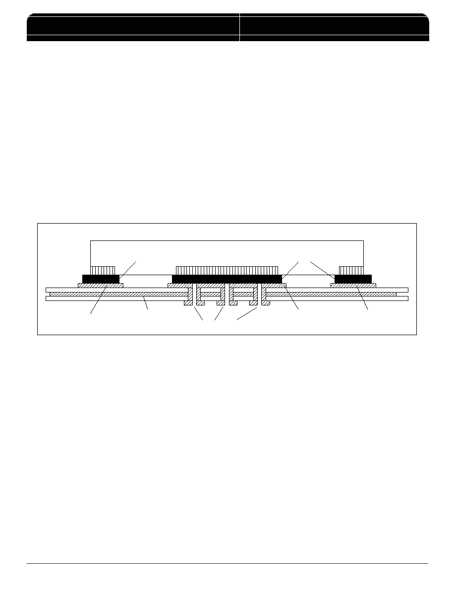
FIGURE 4. P.C.ASSEMBLY FOR EXPOSED PAD THERMAL RELEASE PATH –SIDE VIEW (DRAWING NOT TO SCALE)
VFQFN EPAD THERMAL RELEASE PATH
In order to maximize both the removal of heat from the package
and the electr ical perfor mance, a land patter n must be
incorporated on the Printed Circuit Board (PCB) within the footprint
of the package corresponding to the exposed metal pad or
exposed heat slug on the package, as shown in
Figure 4. The
solderable area on the PCB, as defined by the solder mask, should
be at least the same size/shape as the exposed pad/slug area on
the package to maximize the thermal/electrical performance.
Sufficient clearance should be designed on the PCB between the
outer edges of the land pattern and the inner edges of pad pattern
for the leads to avoid any shorts.
While the land pattern on the PCB provides a means of heat
transfer and electrical grounding from the package to the board
through a solder joint, thermal vias are necessary to effectively
conduct from the surface of the PCB to the ground plane(s). The
land pattern must be connected to ground through these vias.
The vias act as “heat pipes”. The number of vias (i.e. “heat pipes”)
are application specific and dependent upon the package power
dissipation as well as electrical conductivity requirements. Thus,
thermal and electrical analysis and/or testing are recommended
to determine the minimum number needed. Maximum thermal
and electrical performance is achieved when an array of vias is
incorporated in the land pattern. It is recommended to use as
many vias connected to ground as possible. It is also
recommended that the via diameter should be 12 to 13mils (0.30
to 0.33mm) with 1oz copper via barrel plating. This is desirable to
avoid any solder wicking inside the via during the soldering process
which may result in voids in solder between the exposed pad/
slug and the thermal land. Precautions should be taken to
eliminate any solder voids between the exposed heat slug and
the land pattern. Note: These recommendations are to be used
as a guideline only. For further information, refer to the Application
Note on the
Surface Mount Assembly of Amkor’s Thermally/
Electr ically Enhance Leadframe Base Package, Amkor
Technology.
THERMAL VIA
LAND PATTERN
SOLDER
PIN
SOLDER
PIN PAD
PIN
GROUND PLANE
EXPOSED HEAT SLUG
(GROUND PAD)
相关PDF资料 |
PDF描述 |
|---|---|
| LTC1851IFW#PBF | IC ADC 12BIT 1.25MSPS 48-TSSOP |
| LTC1851IFW | IC ADC 12BIT 1.25MSPS 48-TSSOP |
| MS27467T11A35PB | CONN PLUG 13POS STRAIGHT W/PINS |
| LTC1853IFW#PBF | IC A/D CONV 8CH 12BIT 48-TSSOP |
| VE-232-IW-S | CONVERTER MOD DC/DC 15V 100W |
相关代理商/技术参数 |
参数描述 |
|---|---|
| CS5533 | 制造商:CIRRUS 制造商全称:Cirrus Logic 功能描述:16-bit and 24-bit ADCs with Ultra-low-noise PGIA |
| CS5533-AS | 功能描述:模数转换器 - ADC 4-Ch 16-Bit ADCs w/ Ultra Low Noise PGIA RoHS:否 制造商:Texas Instruments 通道数量:2 结构:Sigma-Delta 转换速率:125 SPs to 8 KSPs 分辨率:24 bit 输入类型:Differential 信噪比:107 dB 接口类型:SPI 工作电源电压:1.7 V to 3.6 V, 2.7 V to 5.25 V 最大工作温度:+ 85 C 安装风格:SMD/SMT 封装 / 箱体:VQFN-32 |
| CS5533-ASR | 功能描述:模数转换器 - ADC IC 16-Bit ADCs w/UltraLw Noise PGIA RoHS:否 制造商:Texas Instruments 通道数量:2 结构:Sigma-Delta 转换速率:125 SPs to 8 KSPs 分辨率:24 bit 输入类型:Differential 信噪比:107 dB 接口类型:SPI 工作电源电压:1.7 V to 3.6 V, 2.7 V to 5.25 V 最大工作温度:+ 85 C 安装风格:SMD/SMT 封装 / 箱体:VQFN-32 |
| CS5533-ASZ | 功能描述:模数转换器 - ADC 4-Ch 16-Bit ADCs w/ Ultra Low Noise PGIA RoHS:否 制造商:Texas Instruments 通道数量:2 结构:Sigma-Delta 转换速率:125 SPs to 8 KSPs 分辨率:24 bit 输入类型:Differential 信噪比:107 dB 接口类型:SPI 工作电源电压:1.7 V to 3.6 V, 2.7 V to 5.25 V 最大工作温度:+ 85 C 安装风格:SMD/SMT 封装 / 箱体:VQFN-32 |
| CS5533-ASZ/H1 | 制造商:Cirrus Logic 功能描述: |
发布紧急采购,3分钟左右您将得到回复。